
Method for manufacturing a semiconductor device

a manufacturing method and semiconductor technology, applied in the direction of solid-state devices, transistors, basic electric elements, etc., can solve the problems of gate insulating film characteristics deteriorating, source/drain diffusion layer increasing, and difficult to meet all

Inactive Publication Date: 2006-07-18
KK TOSHIBA
View PDF5 Cites 10 Cited by
  • Summary
  • Abstract
  • Description
  • Claims
  • Application Information

AI Technical Summary

Benefits of technology

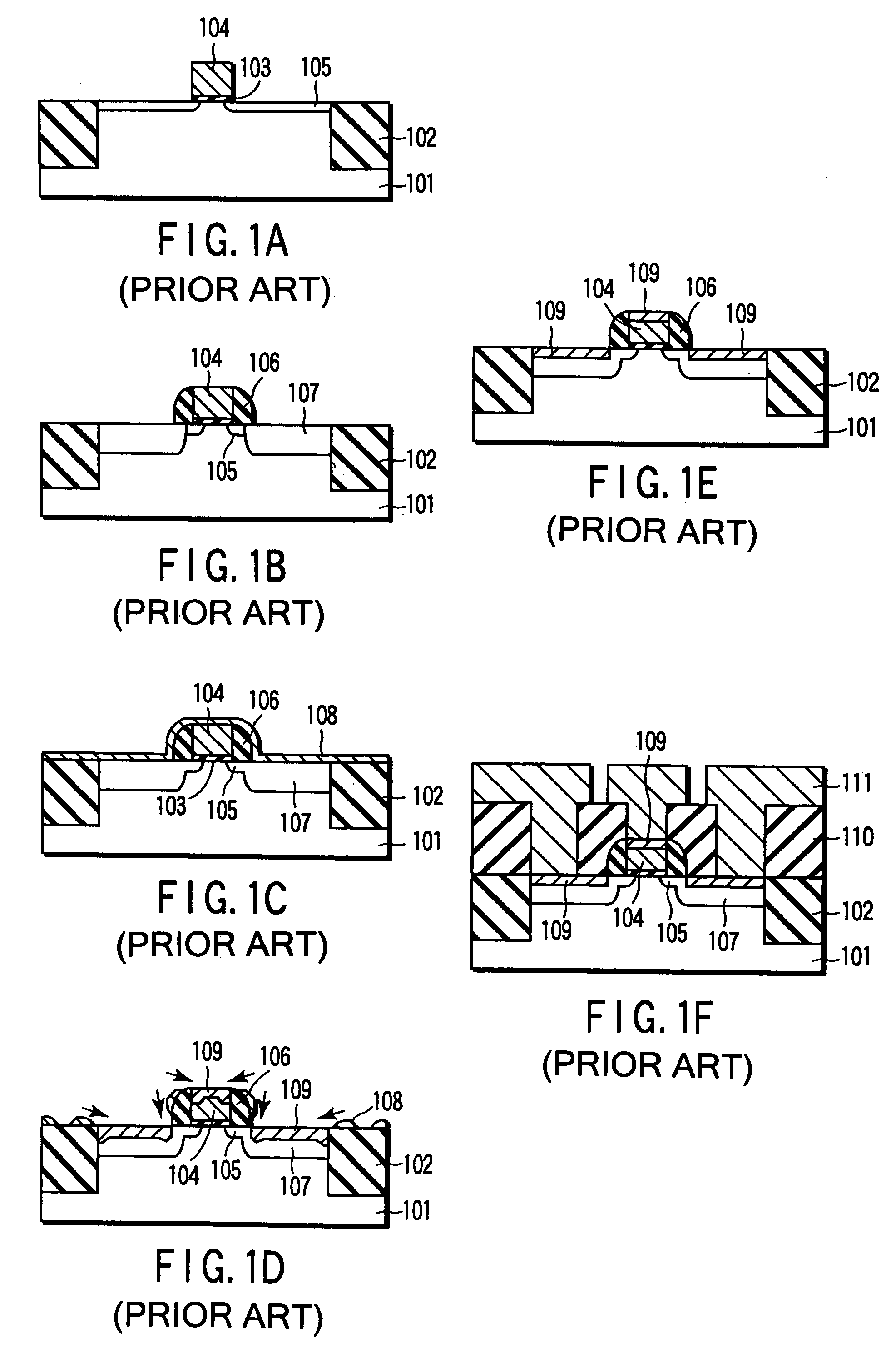
[0042]FIGS. 1A to 1F show respectively a cross-sectional view illustrating in stepwise a manufacturing method of conventional MOS type FET device;
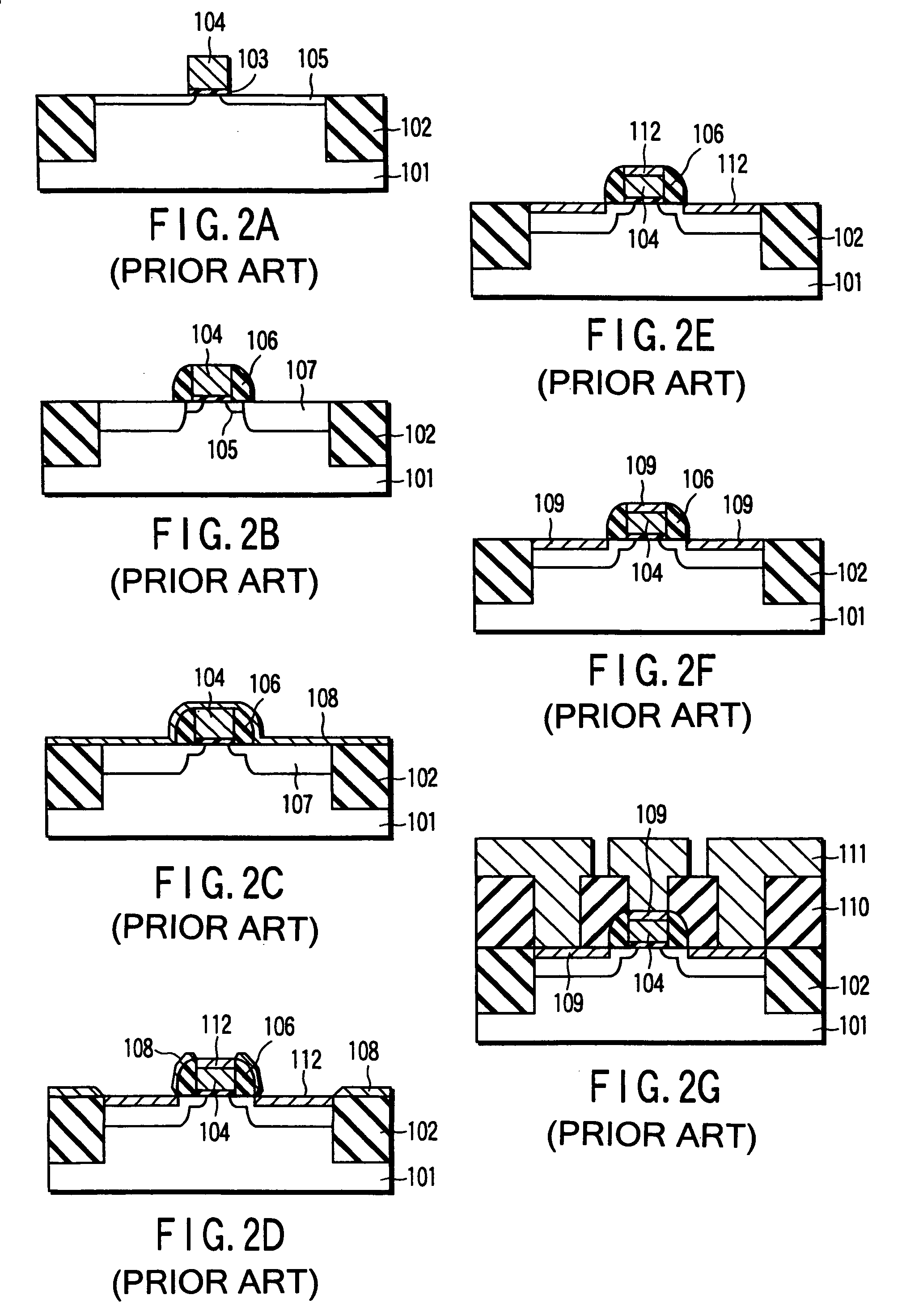
[0043]FIGS. 2A to 2G show respectively a cross-sectional view illustrating in stepwise a manufacturing method of conventional MOS type FET device;
[0044]FIGS. 3A to 3E show respectively a cross-sectional view illustrating the problems accompanied with the conventional manufacturing method of MOS type FET device; and

Problems solved by technology

However, due to the advancement in miniaturization of semiconductor devices these days, it is now considered more difficult to meet all of the aforementioned demands, so that it is now required to employ a nickel silicide (NiSi) film in place of the aforementioned materials.
As a result, problems are raised such that the leak current at the junction (junction leak current) in the source / drain diffusion layer is caused to increase or the characteristics of the gate insulating film is caused to deteriorate.
However, this two-stage heat treatment is accompanied with a problem that when the source / drain diffusion layer or the gate polysilicon electrode contains a high concentration of arsenic impurity, inconveniences are caused to generate in the manufacture of a MOSFET device, thereby making it difficult to manufacture a semiconductor device excellent in reliability.

Method used


Image

  • Method for manufacturing a semiconductor device
  • Method for manufacturing a semiconductor device
  • Method for manufacturing a semiconductor device

Examples


Embodiment Construction

[0046]It has been discovered by the present inventors that when silicon of the diffusion region containing a high-concentration of 1×1020 cm−3 or more of arsenic impurity is reacted with nickel metal to form a nickel silicide film, a large quantity of arsenic atom is permitted to precipitate on the surface of the nickel silicide film, thereby forming an arsenic compound layer.

[0047]Arsenic impurity is frequently introduced into the source / drain diffusion layer or polysilicon electrode of an n-type MOSFET for the purpose of forming a shallow diffusion layer. Particularly in this case, there is a high possibility of causing an arsenic compound layer to precipitate on the surface of the nickel silicide film. Further, due to the arsenic compound layer thus precipitated, the adhesion of an interlayer insulating film deposited on the surface of silicide film is caused to deteriorate. Moreover, when the cleaning treatment of the bottom of contact hole is performed, the arsenic compound lay...


PUM

PropertyMeasurementUnit
temperatureaaaaaaaaaa

Abstract

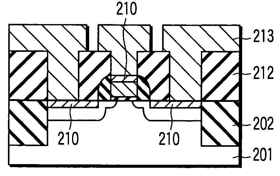
There is disclosed a method of manufacturing a semiconductor device comprising forming a diffusion region containing arsenic impurity at a concentration of 1×1020 cm−3 or more in an element region of Si substrate which is isolated by an element isolating insulation film with a gate electrode being employed as a mask, depositing Ni metal all over the substrate, heat-treating the substrate at a temperature of less than 400° C., thereby forming a nickel silicide film containing Ni2Si on the diffusion region, removing unreacted Ni metal deposited on the element isolating insulation film, heat-treating the substrate at a temperature of 450° C. or more, thereby forming an NiSi film having a arsenic compound layer on the surface thereof, removing the arsenic compound layer by an alkaline liquid, depositing an interlayer insulating film the entire surface of the substrate, and forming a wiring layer piercing through the interlayer insulating film.

Description

CROSS-REFERENCE TO RELATED APPLICATIONS[0001]This application is based upon and claims the benefit of priority from the prior Japanese Patent Application No. 2003-182835, filed Jun. 26, 2003, the entire contents of which are incorporated herein by reference.BACKGROUND OF THE INVENTION[0002]1. Field of the Invention[0003]This invention relates to a method for manufacturing a semiconductor device, and in particular, to a method of forming an MIS (Metal Insulator Semiconductor) type FET (Field Effect Transistor) device wherein a nickel silicide film is formed on a portion of the surface of a contact region of source / drain diffusion layer, and to a method of manufacturing an LSI device comprising the FET device.[0004]2. Description of the Related Art[0005]Concomitant with the advancement in miniaturization of semiconductor devices in recent years, there are persistent demands for the miniaturization of not only the dimension of planes parallel with the surface of semiconductor substrate...

Claims


Application Information

Patent Timeline
Patent Type & Authority Patents(United States)
IPC IPC(8): H01L21/302H01L21/28H01L21/3205H01L21/336H01L23/52H01L29/78
CPCH01L21/28518H01L29/665H01L29/6659H01L29/7833H01L2924/0002H01L2924/00
Inventor IINUMA, TOSHIHIKO
Owner KK TOSHIBA
Learn More