

Chip package and process for forming the same
- Summary
- Abstract
- Description
- Claims
- Application Information
AI Technical Summary
Benefits of technology
Problems solved by technology
Method used
Image

Examples
Embodiment Construction
[0028]Reference will now be made in detail to the present preferred embodiments of the invention, examples of which are illustrated in the accompanying drawings. Wherever possible, the same reference numbers are used in the drawings and the description to refer to the same or like parts.
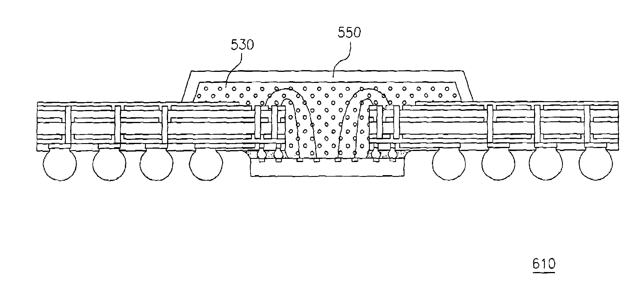
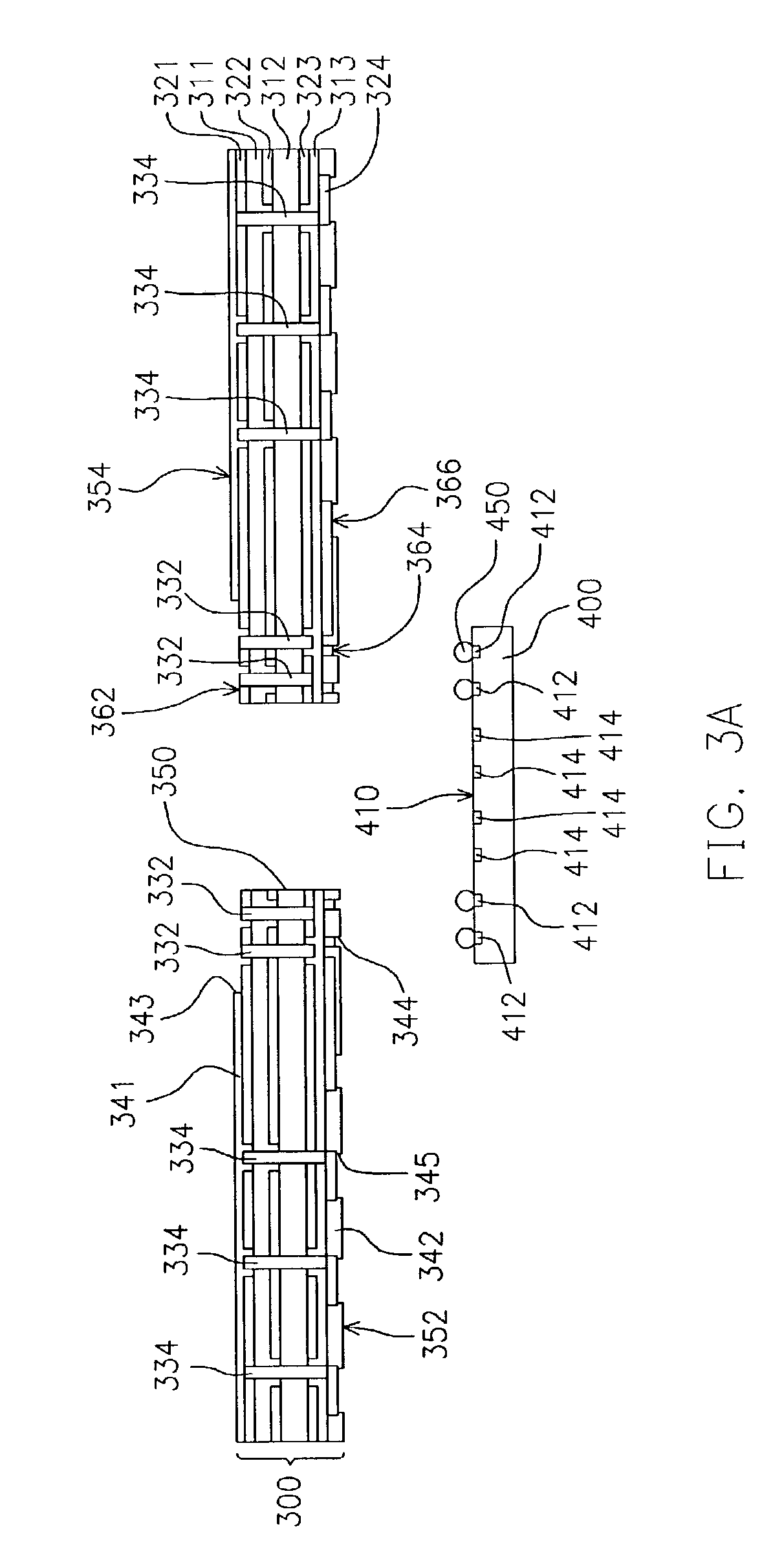
[0029]FIGS. 3A to 3F are schematic cross-sectional views showing the progression of steps for producing a chip package module according to a first preferred embodiment of this invention. As shown in FIG. 3A, a substrate 300 is provided. The substrate 300 comprises three dielectric layers 311, 312, 313 and four patterned metallic layers 321, 322, 323, 324. The patterned metallic layers 321, 322, 323, 324 are sequentially stacked with the dielectric layers 311, 312, 313 positioned between pairs of neighboring patterned metallic layers so that the patterned metallic layers 321, 322, 323, 324 are electrically isolated. Furthermore, the substrate 300 has conductive via plugs 332 and 334. The conductive vi...
PUM
 Abstract
Description
Claims
Application Information