Driving apparatus, driver circuit, and image display apparatus

a driver circuit and image display technology, applied in the direction of electric digital data processing, instruments, computing, etc., can solve the problems of low resistance of output buffers, low reliability of output buffers, and low efficiency of driver construction, so as to reduce the influence of response characteristics of correction circuits and achieve high reliability.

Inactive Publication Date: 2006-07-18
CANON KK
View PDF46 Cites 35 Cited by
  • Summary
  • Abstract
  • Description
  • Claims
  • Application Information

AI Technical Summary

Benefits of technology

[0020]Further, another object of the present invention is to suppress an influence of response characteristics of a correction circuit.
[0021]Also, another object of the present invention is to provide a low-cost driving apparatus with high reliability and an image display apparatus equipped with the same by using a row driver circuit capable of correcting an influence of voltage drop and a column driver circuit appropriate therefor in combination.
[0022]Also, another object of the present invention is to correct the voltage drop due to the resistance disposed outside the driver circuit without involving a complicated structure of the connection portion.
[0038]a column driver circuit adapted to supply to the plurality of column wirings a modulation signal having a pulse width and a voltage amplitude with at least the pulse width modulated according to gradation information, the column driver circuit distributing unit pulse components constituting the modulation signal so as to suppress a change of a current flowing into the selected row wiring in one horizontal scanning period.

Problems solved by technology

When considering the VGA by way of example, the row wiring driver has the outputs as many as 480 channels and thus, high costs are involved when the driver is constructed by discrete devices.
However, taking into consideration the driving of current with several amperes, it is required for an output buffer to have a low ON resistance.
As a result, the number of chips that can be obtained from one wafer decreases, so that unit cost per chip increases.
In particular, this largely affects the IC with the multiple outputs.
However, the inventors have found that only the application of the correction circuit is insufficient to cope with the problems.
Also, due to the resistance at a connection portion where the modulation element is electrically connected with the driver circuit as well, an effective drive voltage actually applied to the modulation element may decrease beyond an allowable range.

Method used


Image

  • Driving apparatus, driver circuit, and image display apparatus
  • Driving apparatus, driver circuit, and image display apparatus
  • Driving apparatus, driver circuit, and image display apparatus

Examples


embodiment 1

(Embodiment 1)

[0171]Referring to FIGS. 7 to 22, a description will be given of a driving apparatus and an image display apparatus provided with the driving apparatus in accordance with Embodiment 1 of the present invention.

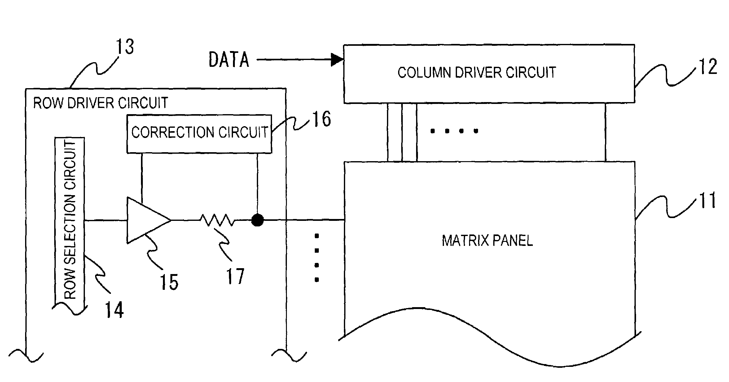
[0172]In this embodiment, as the column driver circuit of a cold cathode display, a circuit that outputs a waveform obtained by using the voltage amplitude modulation and the pulse width modulation in combination is used. The voltage drop of the row selection signal voltage caused by the ON resistance (Ron) of the output transistor in the row driver circuit is corrected by controlling the power source voltage of the row driver circuit through the feedback control by way of example.

[0173]First, referring to FIG. 7, a description will be made of the image display apparatus to which the driving apparatus and the driving method in accordance with the embodiment of the present invention are applied. FIG. 7 is a block diagram showing the driver circuit of the multi-elec...

embodiment 2

(Embodiment 2)

[0237]Another embodiment will be described below. The basic structure is the same as that of Embodiment 1.

[0238]In FIG. 22, a few errors of the row wiring drive voltage output occur in a period B, but more correction errors occur in periods of A and C.

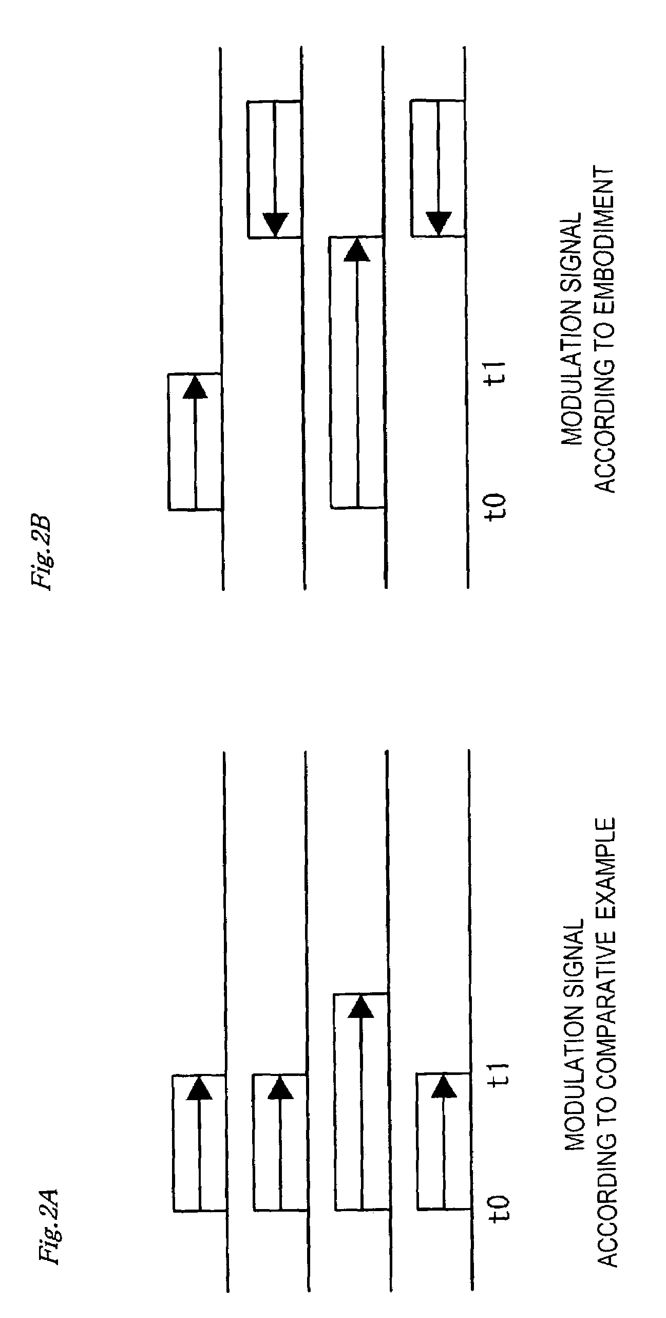
[0239]As shown in FIG. 23, the new Vn drive described above employs a method in which the drive voltage of the row wiring is raised in the amplitude direction sequentially from a waveform 240 to waveforms 241, 242, and 243, in accordance with the inputted drive data. In the period B of FIG. 23, since the change in voltage amplitude is small, the change in current in one horizontal scanning period in the row wiring is extremely small.

[0240]On the other hand, in the periods A and C of FIG. 23, since the change in voltage amplitude becomes large depending on the drive data, the correction error in the periods A and C of FIG. 22 becomes large. To cope with this, it is effective to also cover the Ron correction circuit with a ...

embodiment 3

(Embodiment 3)

[0242]In the embodiments described above, a case is described as an example in which the Ron correction is performed on the multi-output row selection drivers by one operational amplifier 205 serving as common comparison unit. In this embodiment, an operational amplifier 503 is provided for every row wiring drive output as shown in FIG. 26, and inputs potential information of an output terminal of output buffer to a control input terminal 504. With this structure, the gate voltage of an FET 502 is directly driven by the operational amplifier 503 so that an output 501 is constant, and the output is thus corrected.


PUM


Abstract

The present invention can provide a driving apparatus capable of compensating an influence of a voltage drop at low costs in a simple manner, which includes: a column driver circuit that generates at least one of modulation signals different in start reference time in one horizontal scanning period and the modulation signals obtained by using pulse width modulation and voltage amplitude modulation in combination; and a correction circuit that corrects a voltage of the row selection signal so as to suppress a voltage variation of the row selection signal, which is caused due to at least a resistance of an output stage of the row driver circuit and a current caused to flow into the resistance.

Description

BACKGROUND OF THE INVENTION[0001]1. Field of the Invention[0002]The present invention relates to a driving apparatus for a matrix panel used in a monitor of a television receiver, a computer, etc., and an image display apparatus provided with the same. In particular, the invention relates to a driving apparatus for a matrix panel in which modulation elements such as semiconductor light emitting elements and electron emitting elements are arranged at intersections of a matrix, a driver circuit thereof, and an image display apparatus provided with the same.[0003]2. Description of the Related Art[0004]First, a description will be given of the electron emitting element as an example of the modulation element. FIG. 31 schematically shows a matrix panel used for a display apparatus etc.[0005]In FIG. 31, an electron emitting element 1 is schematically shown as an example of the modulation element. A column wiring 2 and a row wiring 3 have wiring resistances 4 and 5 respectively according t...

Claims


Application Information

Patent Timeline
Patent Type & Authority Patents(United States)
IPC IPC(8): G09G5/00G09G3/22G09G3/20G09G3/32
CPCG09G3/2092G09G3/2081G09G2320/0223G09G2310/0267G09G2310/0275G09G3/22
Inventor SHINO, KENJIAOKI, TADASHIISONO, AOJIMURAYAMA, KAZUHIKOSANO, YASUHIKO
Owner CANON KK
Why Eureka
Try Eureka