Magnetoresistive element and magnetoresistive magnetic head, magnetic recording apparatus and magnetoresistive memory device using the same

a technology of magnetic head and magnetic element, which is applied in the direction of nanoinformatics, magnetic bodies, instruments, etc., can solve the problems of insufficient conventional mr element to meet the above demand, non-magnetic layer may affect the degradation, etc., and achieve excellent thermal stability, increase spin polarization, and large mr ratio

Inactive Publication Date: 2006-07-18
PANASONIC CORP
View PDF52 Cites 16 Cited by
  • Summary
  • Abstract
  • Description
  • Claims
  • Application Information

AI Technical Summary

Benefits of technology

[0016]The MR element of the present invention is excellent also in thermal stability. The reason for this is not clarified fully at present, but is considered to be as follows: the addition of the non-magnetic element X reduces the effect of atomic diffusion at the interface between a magnetic layer and a non-magnetic layer and thus stabilizes the interface. The MR element of the present invention is suitable for applications of various devices because of its excellent thermal stability.

Problems solved by technology

Though the reason for degradation of the MR element by heat treatment is not clarified fully at present, diffusion of atoms into the interface between a magnetic layer and a non-magnetic layer may affect the degradation.
However, a conventional MR element is insufficient to meet the above demand.

Method used


Image

  • Magnetoresistive element and magnetoresistive magnetic head, magnetic recording apparatus and magnetoresistive memory device using the same
  • Magnetoresistive element and magnetoresistive magnetic head, magnetic recording apparatus and magnetoresistive memory device using the same
  • Magnetoresistive element and magnetoresistive magnetic head, magnetic recording apparatus and magnetoresistive memory device using the same

Examples


example 1

[0106]Si substrate with a thermal oxide film / Ta(3) / Cu(50) / Ta(3) / Pt—Mn(20) / Co—Fe(1) / ferromagnetic material M-X(2) / Al—O(1.0) / Co—Fe(3) / Ta(15)

[0107]Here, the figures in parentheses denote the film thickness (in nm; the film thickness is expressed in the same manner in the following). The thickness of the Al—O film is a designed thickness (i.e., total thickness) of Al before oxidation (this is the same in the following, including nitridation and oxynitridation for Al—N and Al—N—O). The Al—O was prepared by forming an Al film having a thickness of 0.3 to 0.7 nm and oxidizing the Al film repeatedly in an atmosphere containing oxygen (200 Torr (about 0.267 MPa), 1 min).

[0108]The Ta(3) / Cu(50) on the substrate is a lower electrode, and the Ta(3) adjacent to the Pt—Mn is an underlying layer. The Ta(15) is a protective layer of the MR film, and a portion of the Ta(15) also acts as an upper electrode. The Pt—Mn corresponds to an antiferromagnetic layer. Each film was micro-processed in mesa fash...

example 2

[0115]Si substrate with a thermal oxide film / Ta(3) / Cu(50) / Ta(3) / Pt—Mn(20) / Co—Fe(3) / Ru(0.9) / Co—Fe(1) / ferromagnetic material M-X(2) / Al—O(1.0) / ferromagnetic material M-X(2) / Ni—Fe(5) / Ta(15)

[0116]The method for forming the Al—O film was the same as that in Example 1. Each film was processed in mesa fashion in the same manner as Example 1, and Cu(50) / Ta(3) was formed as an upper electrode. Subsequently, the element was heat-treated at 280° C. for 3 hours in a magnetic field of 5 kOe so as to impart unidirectional anisotropy to the Pt—Mn. The element area of a sample was 2 μm×3 μm.

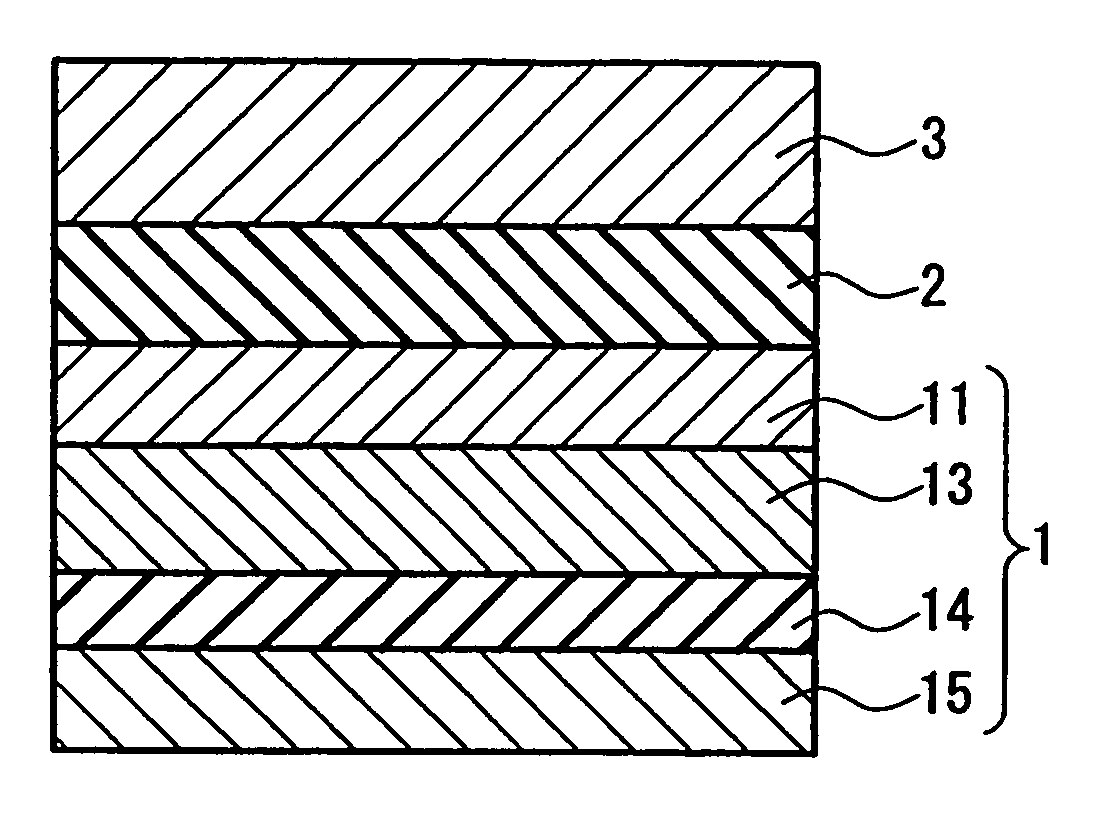
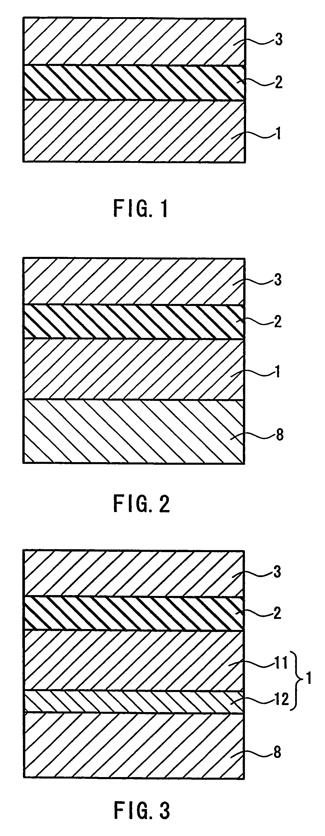
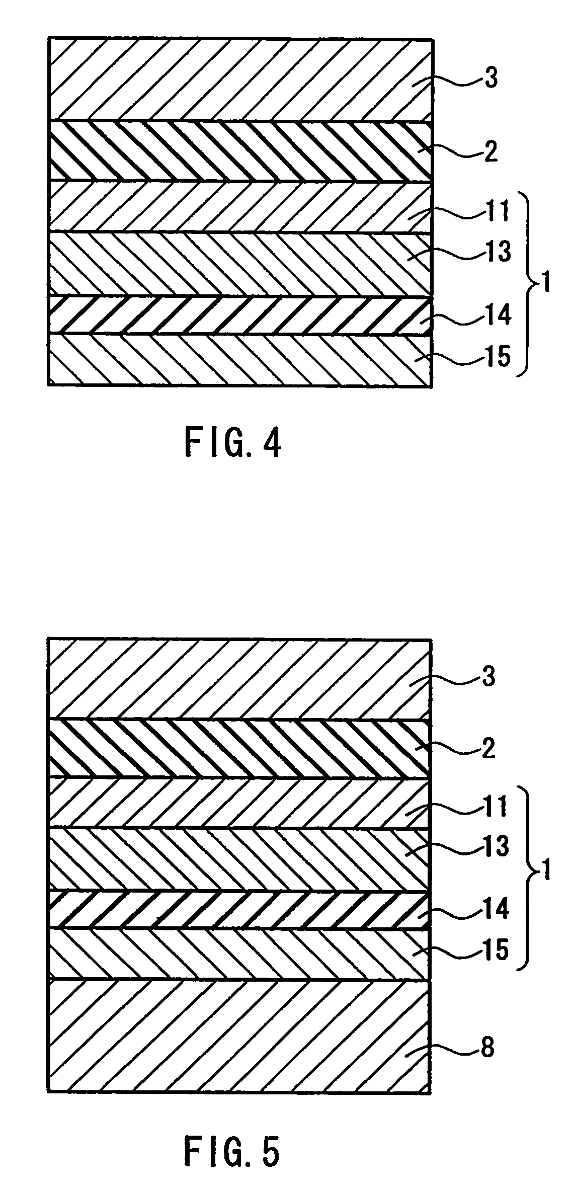
[0117]This MR element is a laminated ferrimagnetic pinned layer spin-valve type TMR element having the configuration in accordance with FIG. 5, and a ferromagnetic material M-X is used for a portion of the pinned layer 1 and a portion of the free layer 3. The free layer 3 includes an Ni—Fe soft magnetic layer. The MR ratio of this element was examined in the same manner as Example 1. Table 2 shows the result.

[011...

example 3

[0121]Si substrate with a thermal oxide film / Ta(3) / Cu(50) / Ta(3) / ferromagnetic material M-X(5) / Al—O(0.8) / Co(3) / Ir—Mn(15) / Ta(20)

[0122]The Al—O was prepared by forming an Al film having a thickness of 0.8 nm and applying ICP oxidation to the Al film. The Ir—Mn corresponds to an antiferromagnetic layer. Each film was processed in mesa fashion in the same manner as Example 1, and Cu(50) / Ta(3) was formed as an upper electrode. Subsequently, the element was heat-treated at 250° C. for 2 hours in a magnetic field of 5 kOe so as to impart unidirectional anisotropy to the Ir—Mn. The element area of a sample was 3 μm×3 μm.

[0123]This MR element is a spin-valve type TMR element having the configuration in accordance with FIG. 2, which is turned upside down, and a ferromagnetic material M-X is used for the free layer 3. The MR ratio of this element was examined in the same manner as Example 1. Table 3 shows the result.

[0124]

TABLE 3Sample No.Ferromagnetic material M-XMR(%)(Conventional example)[Fe...


PUM

PropertyMeasurementUnit
temperatureaaaaaaaaaa
temperaturesaaaaaaaaaa

Abstract

The present invention provides a magnetoresistive (MR) element that is excellent in MR ratio and thermal stability and includes at least one magnetic layer including a ferromagnetic material M-X expressed by M100-aXa. Here, M is at least one selected from Fe, Co and Ni, X is expressed by X1bX2cX3d (X1 is at least one selected from Cu, Ru, Rh, Pd, Ag, Os, Ir, Pt and Au, X2 is at least one selected from Al, Sc, Ti, V, Cr, Mn, Ga, Ge, Y, Zr, Nb, Mo, Hf, Ta, W, Re, Zn and lanthanide series elements, and X3 is at least one selected from Si, B, C, N, O, P and S), and a, b, c and d satisfy 0.05≦a≦60, 0≦b≦60, 0≦c≦30, 0≦d≦20, and a=b+c+d.

Description

[0001]This application is a Continuation of application Ser. No. 10 / 276,966, filed Feb. 19, 2003, abandoned, which is a National Stage application of PCT / JP02 / 04062, filed Apr. 24, 2002, which applications are incorporated herein by reference.TECHNICAL FIELD[0002]The present invention relates to a magnetoresistive element (abbreviated to “MR element” in the following) and magnetic devices using the same. The MR element of the present invention is particularly suitable for a magnetic recording / reproducing head for reading information from media, such as magnetic disks, magneto-optical disks and magnetic tapes, a magnetic sensor used in automobiles or the like, and a magnetoresistive memory device (i.e., a magnetic random access memory, abbreviated to “MRAM” in the following).BACKGROUND ART[0003]A multi-layer film in which at least two magnetic layers and at least one non-magnetic layer are stacked alternately can provide a large magnetoresistance effect, which is called a giant magne...

Claims


Application Information

Patent Timeline
Patent Type & Authority Patents(United States)
IPC IPC(8): G11B5/127G01R33/09G11B5/39H01F10/14H01F10/16H01F10/32H01L21/8246H01L27/105H01L43/08H01L43/10
CPCB82Y10/00B82Y25/00G01R33/093G11B5/3903G11B5/3909G11B5/3916H01F10/3204H01F10/3231H01F10/3254H01F10/3268H01L43/10H01F10/3295Y10T428/115G11B2005/3996H10N50/85
Inventor SUGITA, YASUNARIHIRAMOTO, MASAYOSHIMATSUKAWA, NOZOMUSATOMI, MITSUOKAWASHIMA, YOSHIOODAGAWA, AKIHIRO
Owner PANASONIC CORP
Why Eureka
Try Eureka