Method for analyzing power noise and method for reducing the same

a power noise and power noise technology, applied in noise figures or signal-to-noise ratio measurement, instruments, electric devices, etc., can solve problems affecting the operation performance of ic and signal accuracy, and achieve the effects of reducing power noise, power noise reduction, and voltage variation and power nois

Inactive Publication Date: 2006-07-18
SILICON INTEGRATED SYSTEMS
View PDF8 Cites 10 Cited by
  • Summary
  • Abstract
  • Description
  • Claims
  • Application Information

AI Technical Summary

Benefits of technology

[0008]It is the principal object of the present invention to provide a method for analyzing power noise and a method for reducing the power noise. In the IC design process, by defining the power network of a IC layout constructed by many unit blocks, and according to the parameters, such as type and quantity, etc., of components, such as clock buffers, logic components and logic circuits (i.e. D-Flip-Flop) used for constructing clock tree and clock transmission, electrically connected to each of the unit blocks, the power noise and voltage drop caused in operation of each of the unit blocks can be evaluated, so that appropriate capacitors can be placed on proper locations of IC for compensating the voltage drop and decreasing the voltage variation and power noise.
[0009]In accordance with the aforementioned purpose of the present invention, the present invention provides a method for analyzing power noise and a method for reducing the same. First, by utilizing computer aided design (CAD) software, a chip power analysis is performed with related IC design data for obtaining a power network model of IC design. Then, the power network model is defined as being constructed by many unit blocks interconnected with each other. After analyzing the related data of IC design, the parameters, such as type and quantity, etc., of components electrically connected to each of the unit blocks are resolved and obtained and regarded as a component reference data of each of the unit blocks. Afterwards, according to each component reference data of each of unit blocks, the voltage drop caused by each of the unit blocks in operation is evaluated by utilizing an equivalent circuit constructed by components that are connected electrically to each of the unit blocks. Therefore, the consumption and distribution of voltage in each region of the power network model are obtained, so as to place appropriate capacitors in proper locations of the power network model, in order to compensate the voltage drop caused by components of IC in operation, and to decrease the power noise in the IC.

Problems solved by technology

In the view of the background of the invention described above, since the operation frequency of IC currently used is getting higher, and the area of chip is also increased due to the technology progresses of semiconductor process and IC design, the voltage drop caused by semiconductor components of IC in operation becomes bigger, and meanwhile, the high operation frequency of semiconductor components generates sever power noise that interferes and pollutes the regular operation signals of circuit and power supply, thus affecting the operation performance of IC and the signal accuracy.

Method used


Image

  • Method for analyzing power noise and method for reducing the same
  • Method for analyzing power noise and method for reducing the same
  • Method for analyzing power noise and method for reducing the same

Examples


Embodiment Construction

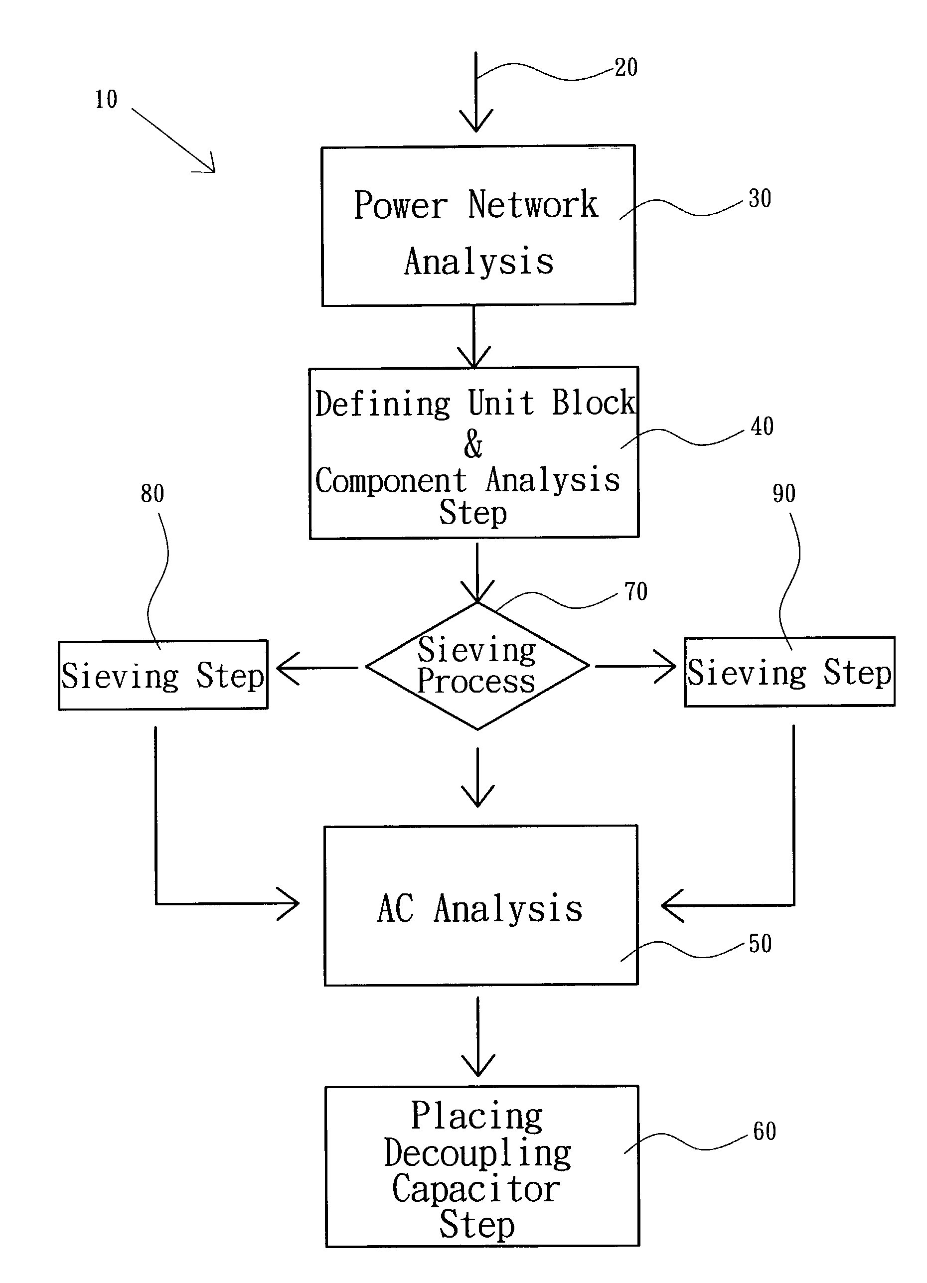
[0014]Please referring to FIG. 1, FIG. 1 is a flow chart showing a process of a preferred embodiment of the present invention. As shown in FIG. 1, in order to obtain a power network model of an IC design, related design reference data 20 of IC design are first inputted in the power network analysis 30 of the process flow 10. By utilizing the computer aided design software, a chip power analysis is performed for obtaining the power network model of IC design. According to the power network model of IC design, the related reference data, characteristics and parameters of a DC power network model and an AC power network model of IC design can be obtained, wherein the related reference data of IC design comprises: standard component library, impedance of power network, operation frequency, operation temperature range, temperature coefficient, voltage drop range, each length and width of the metal lines in each metal layer of the power network, distance between metal lines and other rela...


PUM


Abstract

A method for analyzing power noise and method for reducing the same are disclosed, wherein the present invention is utilized in an IC design process. First, a DC analysis is performed with a related IC design by utilizing computer aided design (CAD) software and circuit simulation software for obtaining a power network model of the IC design. Then, the power network model is defined as being composed of a plurality of unit blocks. After analysis, the quantity and type, etc., of components connected electrically to each of the unit blocks are recognized and are regarded as component reference data of each of the unit blocks. Afterwards, according to the component reference data of each of the unit blocks, the voltage drop (IR drop) occurring in operation for each of the unit blocks is evaluated and obtained by utilizing an equivalent circuit constructed by components that are connected electrically to each of the unit blocks. Therefore, the voltage consumption and distribution in each region of the power network model are obtained, so that at least one appropriate capacitor can be placed on proper locations of the power network model, to compensate the voltage drop caused by the IC design components while in operation, and to decrease the power noise in the IC design.

Description

FIELD OF THE INVENTION[0001]The present invention relates to a method for analyzing power noise and method for reducing the same, and more particularly relates to a method for analyzing power noise and method for reducing power noise in an IC design process by placing appropriate capacitors on IC properly, in order to decrease the power noise in the IC.BACKGROUND OF THE INVENTION[0002]With the technologies of semiconductor process and IC design continuously progressing, ICs with different functions are widely utilized in various products. Meanwhile, the critical dimension of semiconductor components is advanced to a scope of sub-microns, and even to that of deep sub-microns, so that the integrity of IC is increased rapidly. Since there is no sufficient area on the surface of semiconductor structure for producing the interconnections required by semiconductor components, the technique of multilevel interconnection is developed to perform the interconnection and insulation among semic...

Claims


Application Information

Patent Timeline
Patent Type & Authority Patents(United States)
IPC IPC(8): G06F17/50H01L25/00G01R29/26
CPCG01R29/26G06F30/367G06F2119/06
Inventor TIEN, HAO-LUENCHEN, SHANG-YILU, MING-HUANTU, CHUN-AN
Owner SILICON INTEGRATED SYSTEMS
Why Eureka
Try Eureka