Polishing method and apparatus

a technology of polishing method and polishing machine, which is applied in the direction of lapping machine, grinding machine components, manufacturing tools, etc., can solve the problems of thinning, dishing, erosion, and thinning, and the inability to achieve micro-planarization

Inactive Publication Date: 2006-07-25
CANON KK
View PDF5 Cites 15 Cited by
  • Summary
  • Abstract
  • Description
  • Claims
  • Application Information

AI Technical Summary

Benefits of technology

[0019]According to the present invention, it is possible to provide a polishing method and apparatus suitable for measurement of a mark previously formed on a substrate.

Problems solved by technology

However, the grid-like groove pattern in the surface of the polishing pad P is transferred to the polished surface of the wafer W, thus making it impossible to achieve micro-planarization.
Further, in a CMP apparatus, polishing is effected with a viscoelastic polishing pad, such as a polyurethane pad, so that, due to deformation of the polishing pad during polishing, the portions where the projections and depressions are not dense are not polished flat, resulting in so-called dishing, erosion, and thinning.
However, the configuration of the measurement mark for alignment measurement and overlay inspection measurement is under the influence of dishing, erosion, and thinning, and the size of the measurement mark is relatively large, in particular, in width, as compared with the device pattern, which leads to a difference in the peripheral pattern density, resulting in over-polishing or the like.
As a result, the configuration of the measurement mark becomes asymmetrical, which leads to a deterioration in accuracy in alignment and overlay inspection.
At this time, the reflection angles of the lights reflected from the right and left sides of the measurement mark AM differ, so that the video signal is also asymmetrical, which leads to distortion, resulting in positional deviation.
This leads to a deterioration in alignment accuracy and overlay inspection accuracy.
However, due to the recent rapid progress in the microfabrication technique for semiconductor devices, it has become impossible to meet the requisite level of alignment accuracy and overlay inspection accuracy even through polishing while controlling the rotating speed of the semiconductor substrate and / or the polishing pad.
In other words, while the control of the rotating speed of the semiconductor substrate and / or the polishing pad makes it possible to mitigate asymmetrical polishing of the film on the measurement mark, it does not enable the film on the measurement mark to be polished symmetrically but allows generation of slight asymmetric diversity.

Method used


Image

  • Polishing method and apparatus
  • Polishing method and apparatus
  • Polishing method and apparatus

Examples


Embodiment Construction

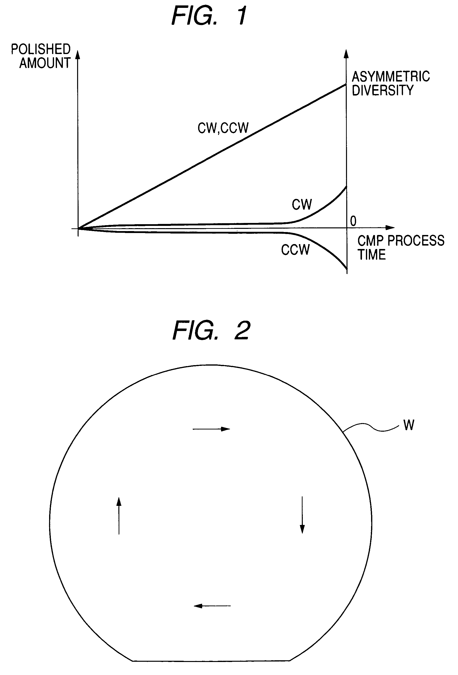
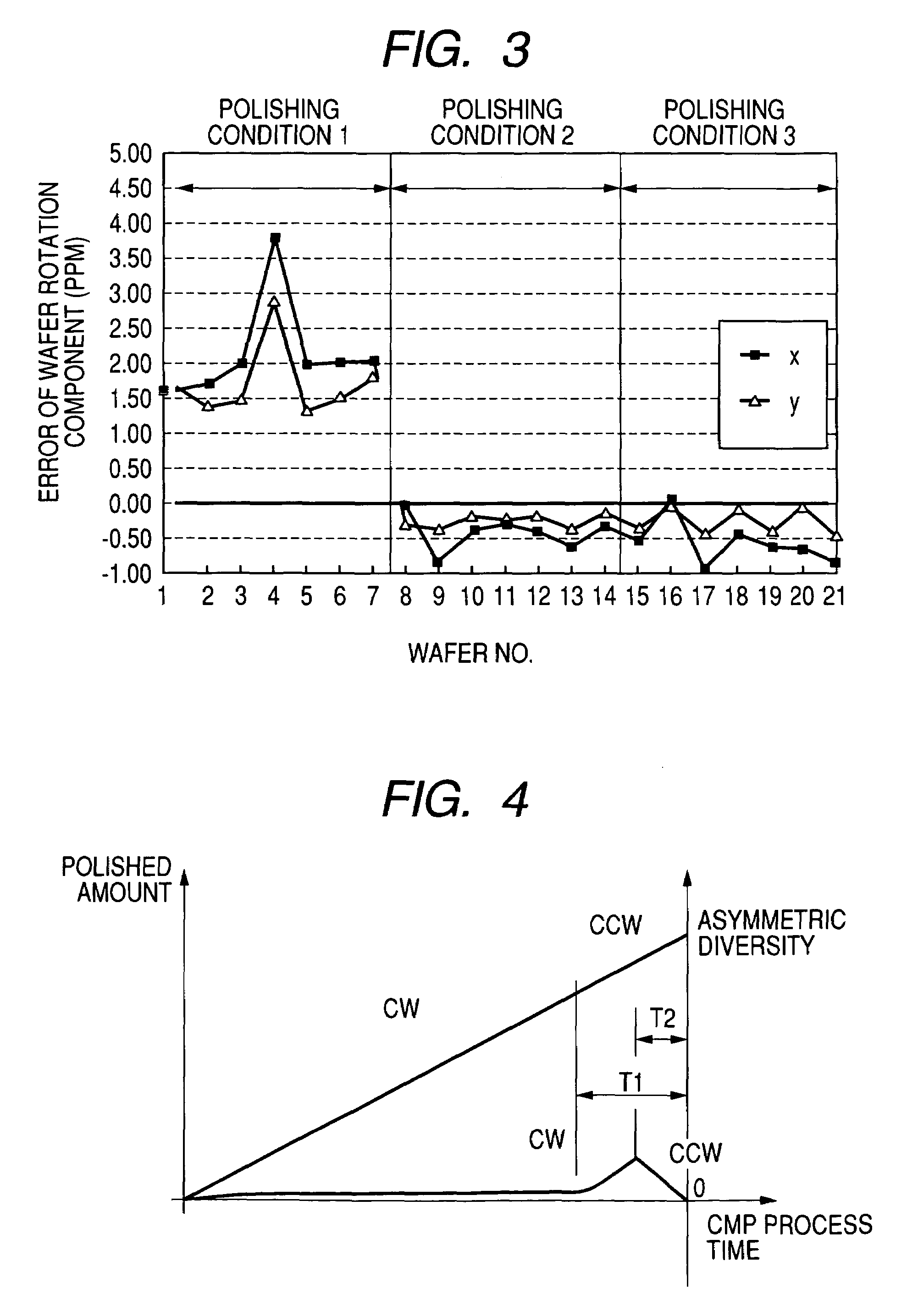
[0041]In providing a polishing method and a polishing apparatus making it possible to polish a film on a measurement mark for positioning or the like with projections and depressions into a symmetrical configuration, the inventor of the present invention, going back to the basics, has carefully examined the asymmetric diversity of the film on the measurement mark generated by polishing, and has found out that when, in a CMP apparatus, the rotational direction of the wafer and the polishing pad is reversed, the asymmetric diversity of the film on the measurement mark after CMP is also reversed. Further, the inventor has found out that the CMP polished amount is proportional to the polishing time irrespective of the rotational direction of the wafer and the polishing pad. Further, the inventor has found out that the asymmetric diversity of the film on the measurement mark is only generated during the last section of the entire polishing time.

[0042]FIG. 1 is a graph showing the relatio...


PUM

PropertyMeasurementUnit
sizeaaaaaaaaaa
sizeaaaaaaaaaa
sizeaaaaaaaaaa

Abstract

Provided is a polishing method of polishing a substrate by rotating the substrate and a pad while keeping the pad in contact with the substrate, the method including: a first polishing step of polishing the substrate by rotating the substrate and the pad in a first direction; and a second polishing step of polishing the substrate by rotating the substrate and the pad in a second direction opposite to the first direction.

Description

BACKGROUND OF THE INVENTION[0001]1. Field of the Invention[0002]The present invention generally relates to a polishing method and apparatus. In particular, the present invention relates to a polishing method and apparatus for semiconductor wafers of Si, GaAs, InP, etc. and substrates, such as quartz substrates and glass substrates with a plurality of island-like semiconductor regions formed on the surfaces thereof.[0003]2. Related Background Art[0004]With progress in microfabrication of semiconductor devices, there are needs for highly precise planarization of outer surfaces of semiconductor wafers of Si, GaAs, InP, etc. and substrates, such as quartz substrates and glass substrates on the surface of which a plurality of island-like semiconductor regions are formed. Further, global planarization of the outer surfaces of substrates is also demanded due to the emergence of SOI wafers and the necessity for three-dimensional integration.[0005]In addition to such global planarization of ...

Claims


Application Information

Patent Timeline
Patent Type & Authority Patents(United States)
IPC IPC(8): B24B49/00B24B37/10B24B49/12H01L21/304
CPCB24B49/12B24B37/042
Inventor INA, HIDEKI
Owner CANON KK
Why Eureka
Try Eureka