
Electronic component value trimming systems

a technology of electronic components and trimming systems, applied in logic circuit coupling/interface arrangements, pulse techniques, instruments, etc., can solve the problems of static power consumption of many conventional systems, low power application problems, and high cost, and achieve the effect of eliminating cross talk and noise coupling between networks

Inactive Publication Date: 2006-07-25
IBM CORP
View PDF11 Cites 14 Cited by
  • Summary
  • Abstract
  • Description
  • Claims
  • Application Information

AI Technical Summary

Benefits of technology

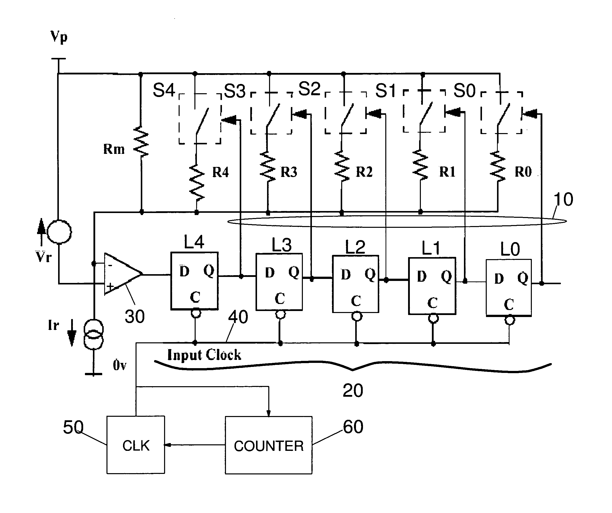
The present invention provides a system for trimming the value of an electronic component by selectively connecting trimming components to the electronic component in dependence on a control vector. The system includes a controller with a shift register for sequentially receiving output bits from a comparator and generating the control vector accordingly. The trimming components can be resistors, capacitors, or inductors, and can be connected in parallel or series with the electronic component. The system compensates for tolerance in integrated electronic components, providing a more accurate value than could be obtained without compensation. The resistance value set by the system can be defined primarily by the value of a reference resistor and is independent of other variables. The system also allows for effective elimination of cross talk and noise coupling between networks.

Problems solved by technology

Many conventional systems have the disadvantage of static power consumption.
This can be particularly problematical in low power applications.
In addition, where such systems involve the distribution of an analogue voltage signal, there can be susceptibility to interference and error.
In this design, there is also significant overhead in the system control logic.
This overhead is a disadvantage for applications in which there are multiple components to be trimmed on an IC.
The latter may involve complex routing of a control bus across the IC.
The control bus may have many bits, further complicating such routing.

Method used


Image

  • Electronic component value trimming systems
  • Electronic component value trimming systems
  • Electronic component value trimming systems

Examples


Embodiment Construction

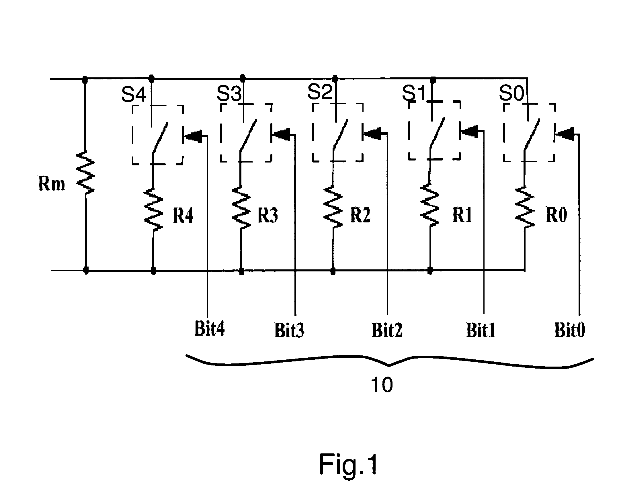
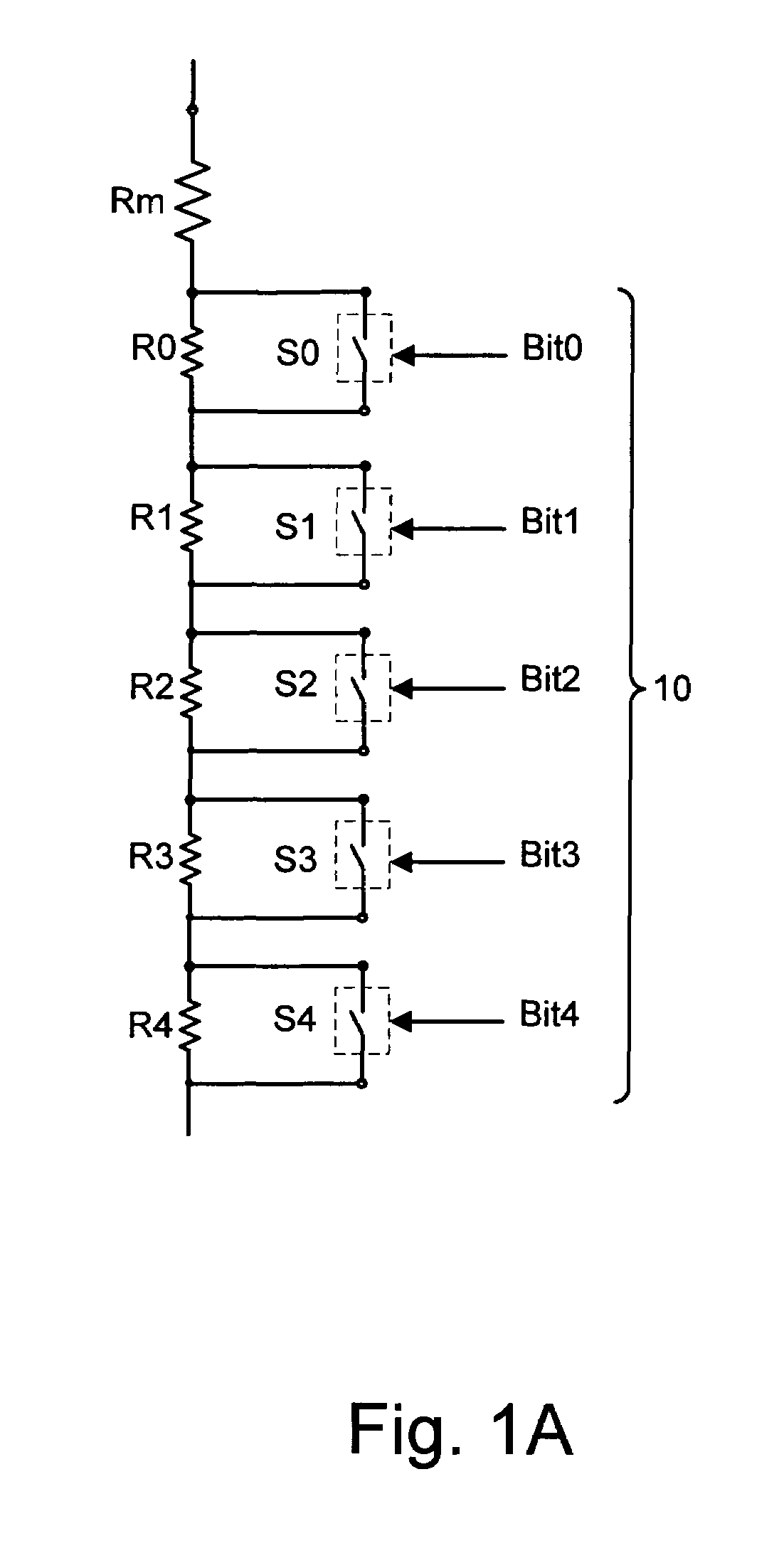
[0027]Referring to FIG. 1, in a preferred embodiment of the present invention, there is provided a network comprising a main resistor Rm and plural parallel trimming resistors R0–R4 each selectively connectable in parallel with the main resistor Rm via a corresponding one of a plurality of series switches S0–S4. The trimming resistors R0–R4 are employed to compensate for the tolerance of the main resistor Rm. The trimming resistors R0–R4 may be switched in or out of circuit by a digital control vector 10. The control vector has 5 bits, Bit0–Bit4. Each bit is applied to a control electrode of a different one of the switches S0–S4. In other embodiments of the present invention, the control vector 10 may have more than or less than 5 bits. The switches S0–S4 may be conveniently implemented by transistor switches. In a particularly preferred embodiment of the present invention, the switches S0–S4 are each implemented by a field effect transistor having a channel connected in series with...


PUM


Abstract

Described is a system for trimming the value of an electronic component. The system comprises: at least one trimming component, each trimming component having an associated switch for selectively connecting that trimming component to the electronic component in response to a corresponding bit in a control vector. A comparator is included for generating an output bit having a first value if a net value of the electronic component and any connected trimming components differs from a desired value. A controller connected to the switches and the comparator generates the control vector in dependence on the output of comparator, the controller comprising a shift register for sequentially receiving successive output bits from the comparator; wherein the control vector comprises the contents of the shift register and wherein a bit of said first value in control vector effects switching of the corresponding switch.

Description

BACKGROUND OF THE INVENTION[0001]1. Field of the Invention[0002]The present invention generally relates to electronic component value trimming systems and particularly relates to a system for trimming the effective value of an electronic component such as a resistor in an integrated circuit (IC) to a desired value.[0003]2. Description of the Related Art[0004]Conventional techniques for trimming the effective value of an electronic component to a desired or target value comprise selectively connecting a main component to one or more trimming components via a network of switchable interconnections. Such systems can compensate for the tolerance of IC components such as resistors and provide a more accurate value than possible with an uncompensated component. There are applications where well controlled IC resistor networks are desirable. One such application, for example, is in the termination of transmission lines to optimise signal quality.[0005]Many conventional systems have the dis...

Claims


Application Information

Patent Timeline
Patent Type & Authority Patents(United States)
IPC IPC(8): H03M1/10H01C17/22
CPCH01C17/22
Inventor CRANFORD, JR., HAYDEN CLAVIEHSU, LOUIS LU-CHENMASON, JAMES STEPHENNICHOLLS, GARETH JOHNMURFET, PHILIPRAY, SAMUEL
Owner IBM CORP
Learn More