

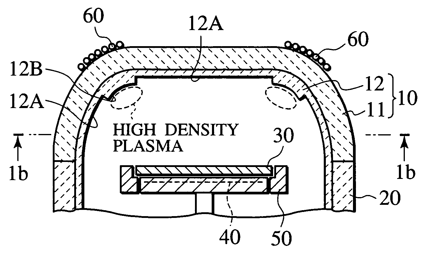
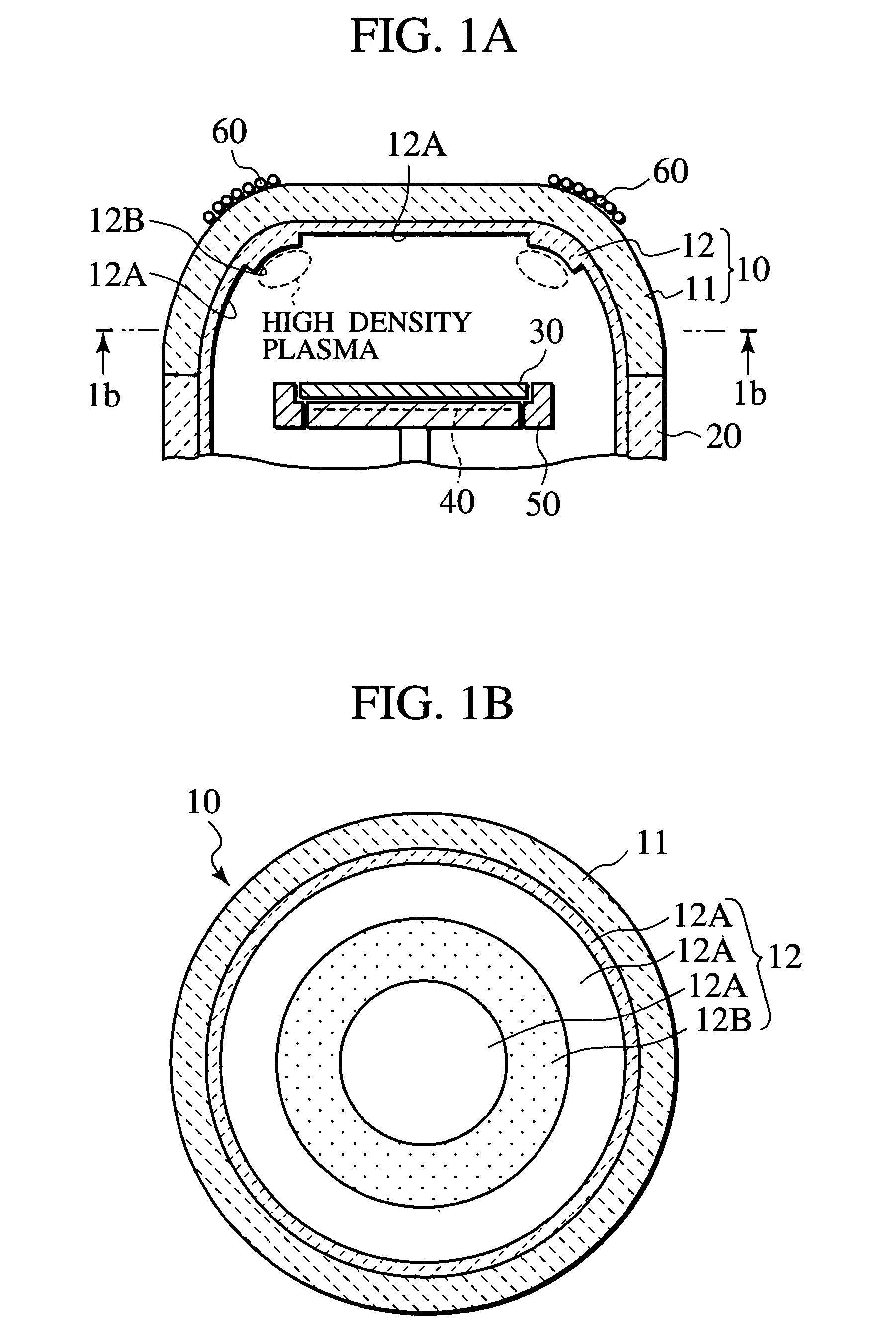
Ceramic member
- Summary
- Abstract
- Description
- Claims
- Application Information
AI Technical Summary
Benefits of technology
Problems solved by technology
Method used
Image

Examples
examples
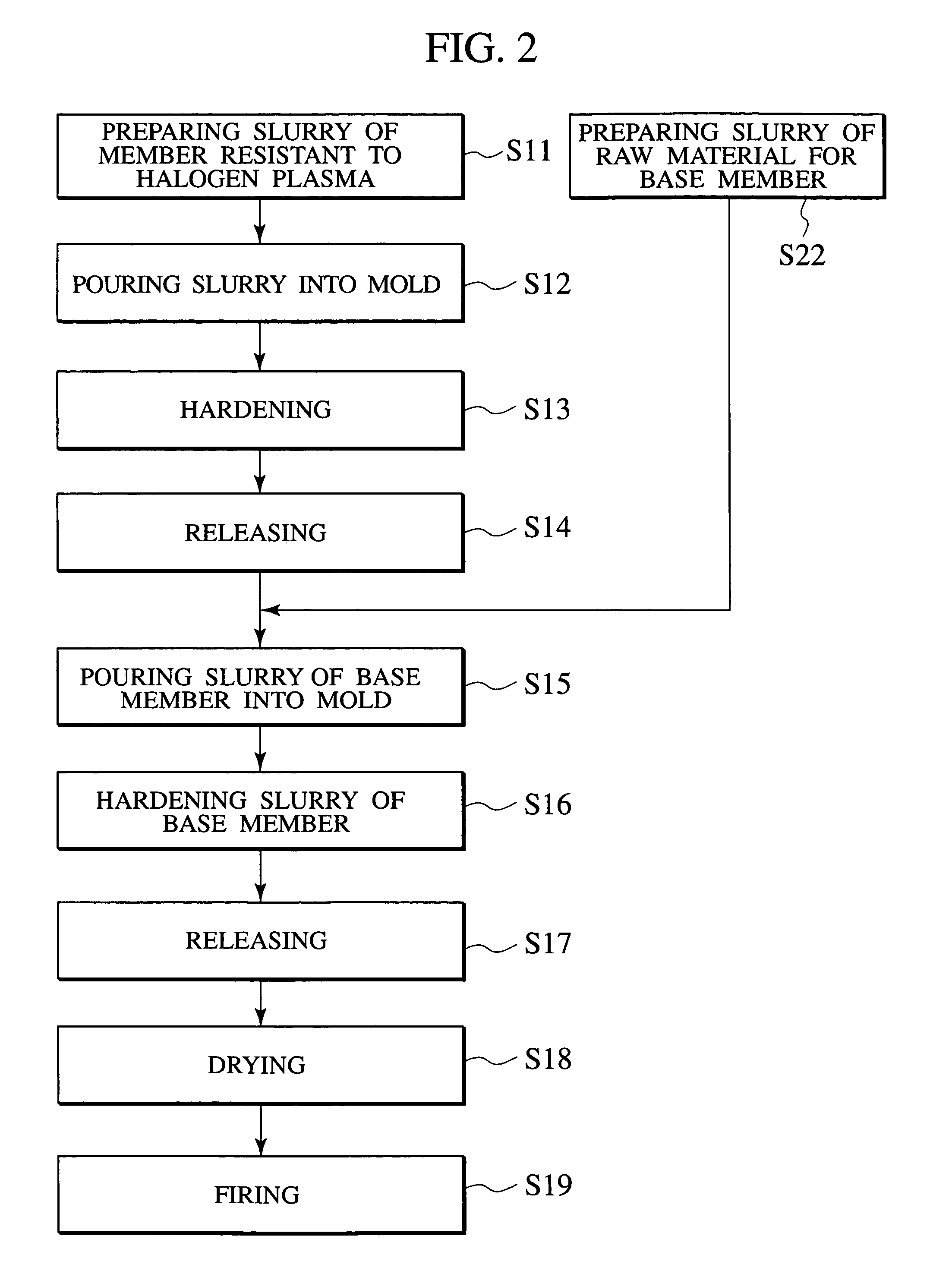
[0060]Studied examples made for realizing effects of the present invention will be described below.
[0061]As shown in FIG. 5, a member sample 310 in which a coating layer 312 composed of a YAG sintered body was formed on one surface of a base member 311 composed of a disc-shaped alumina sintered body with a diameter of 300 mm was prepared under the following conditions. On the coating layer 312, a ring-shaped thick portion 312B with an inner diameter of 100 mm and an outer diameter of 150 mm was formed.
[0062]Note that, for an area, thickness of a normal thickness portion 312A and thickness of the thick portion 312B of the coating layer 312, conditions shown in Table 1 were used.
[0063]First, 100 parts by weight of YAG powder, 25 parts by weight of dimethyl glutanate that was a dispersing medium, 6 parts by weight of hexamethylene-diisocyanate that was a binder, and 2 parts by weight of copolymer of polymaleic acid that was a dispersant were mixed, and 4.5 parts by weight of triethylam...
PUM
| Property | Measurement | Unit |
|---|---|---|
| Thickness | aaaaa | aaaaa |
| Thickness | aaaaa | aaaaa |
| Thickness | aaaaa | aaaaa |
Abstract
Description
Claims
Application Information