
Method of forming a via hole through a glass wafer

Active Publication Date: 2006-08-01
SAMSUNG ELECTRONICS CO LTD
View PDF9 Cites 79 Cited by
  • Summary
  • Abstract
  • Description
  • Claims
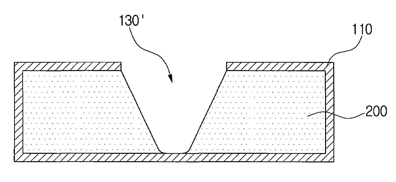
  • Application Information

AI Technical Summary

Benefits of technology

[0008]Accordingly, the present invention has been made in an effort to solve at least some of the above-mentioned problems occurring in the prior art. A feature of the present invention is to provide a method of forming a via hole through a glass wafer in an MEMS packaging that is capable of preventing formation of an undercut and minute cracks at the via hole and enables the via hole to have a smooth surface.
[0009]To provide this feature, an embodiment of the present invention provides a method of forming a via hole through a glass wafer including depositing a material layer on an outer surface of the glass wafer, the material layer having a selection ratio higher than that of the glass wafer, forming a via-patterned portion on one side of the material layer, performing a first etching in which the via-patterned portion is etched to form a preliminary via hole, eliminating any remaining patterning material used in the formation of the via-patterned portion, performing a second etching in which the preliminary via hole is etched to form a via hole having a smooth surface and extending through the glass wafer, and eliminating the material layer.

Problems solved by technology

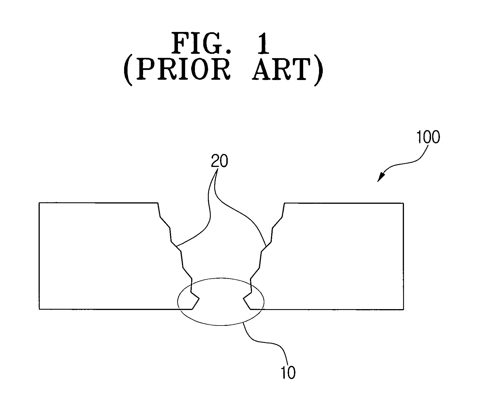
In a conventional method of forming a via hole in a wafer level, however, since the via hole is formed by sandblasting after being patterned on a surface of the glass wafer, it is problematic in that the formed via hole may have an undercut portion and a rough surface.
This undercut problem is especially pronounced in the formation of a via hole having a small diameter.
In this case, not only is it difficult to etch the via hole, but the formed via hole may also have an undercut portion that causes a severe problem.
In the case of the method employing the CMP step, however, since a portion of the glass surface is completely eliminated, characteristics of elements may be damaged in a packaging in which the delicate glass surface plays an important role.
Further, the method employing the deposition of a metal film requires increased manufacturing steps and manufacturing cost.
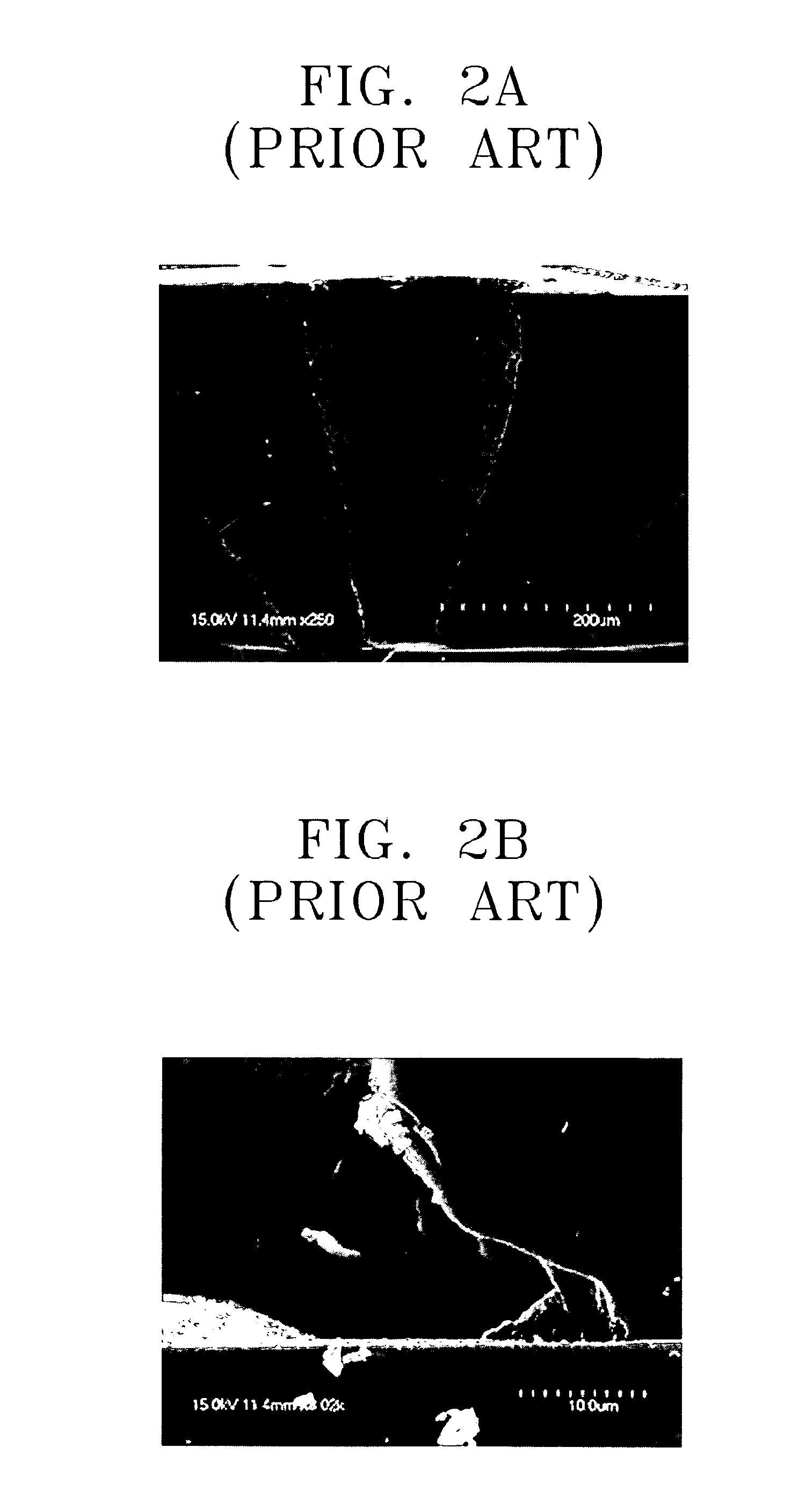
Moreover, when the via hole is formed by sandblasting, the via hole may not only have a rough surface, but may also have minute cracks formed therein.

Method used


Image

  • Method of forming a via hole through a glass wafer
  • Method of forming a via hole through a glass wafer
  • Method of forming a via hole through a glass wafer

Examples


Embodiment Construction

[0020]Korean Patent Application No. 2002-70121, filed on Nov. 12, 2002, and entitled: “Method of Forming a Via Hole Through a Glass Wafer,” is incorporated by reference herein in its entirety.

[0021]The present invention will now be described more fully hereinafter with reference to the accompanying drawings, in which a preferred embodiment of the invention is shown. The invention may, however, be embodied in different forms and should not be construed as limited to the embodiments set forth herein. Rather, these embodiments are provided so that this disclosure will be thorough and complete, and will fully convey the scope of the invention to those skilled in the art. In the drawings, the thickness of layers and regions are exaggerated for clarity. It will also be understood that when a layer is referred to as being “on” another layer or substrate, it can be directly on the other layer or substrate, or intervening layers may also be present. Like numbers refer to like elements throug...


PUM

PropertyMeasurementUnit
Electrical resistanceaaaaaaaaaa
Ratioaaaaaaaaaa
Depthaaaaaaaaaa

Abstract

A method of forming a via hole through a glass wafer includes depositing a material layer on an outer surface of the glass wafer, the material layer having a selection ratio higher than that of the glass wafer, forming a via-patterned portion on one side of the material layer, performing a first etching in which the via-patterned portion is etched to form a preliminary via hole, eliminating any remaining patterning material used in the formation of the via-patterned portion, performing a second etching in which the preliminary via hole is etched to form a via hole having a smooth surface and extending through the glass wafer, and eliminating the material layer. The method according to the present invention is able to form a via hole through a glass wafer without allowing formation of an undercut or minute cracks, thereby increasing the yield and reliability of MEMS elements.

Description

BACKGROUND OF THE INVENTION[0001]1. Field of the Invention[0002]The present invention relates to a method of forming a via hole through a glass wafer. More particularly, the present invention relates to a method of forming a via hole through a glass wafer without producing an undercut.[0003]2. Description of the Related Art[0004]It is generally known in the art that a via hole (or simply a “via”) necessarily should be formed in a wafer level of a micro-electromechanical system (MEMS) packaging utilizing glass to permit the electrical processing of elements in the MEMS. In a conventional method of forming a via hole in a wafer level, however, since the via hole is formed by sandblasting after being patterned on a surface of the glass wafer, it is problematic in that the formed via hole may have an undercut portion and a rough surface. This undercut problem is especially pronounced in the formation of a via hole having a small diameter. In this case, not only is it difficult to etch t...

Claims


Application Information

Patent Timeline
IPC IPC(8): H01L21/302B81B1/00B81C1/00H01L21/84
CPCB81C1/00087H01L21/486H01L23/13H01L2924/0002H01L2924/00H01L21/84
Inventor LEE, MOON-CHULCHOI, HYUNGJUNG, KYU-DONGJANG, MIHONG, SEOG-WOOCHUNG, SEOK-WHANJUN, CHAN-BONGKANG, SEOK-JIN
Owner SAMSUNG ELECTRONICS CO LTD
Learn More