

Plasma display panel
a technology of display panels and plasma, which is applied in the direction of discharge tube main electrodes, discharge electrodes, gas-filled discharge tubes, etc., can solve the problems of increasing wiring resistance, and achieve the effect of stable electrode wiring characteristics and highly reliable pdp
- Summary
- Abstract
- Description
- Claims
- Application Information
AI Technical Summary
Benefits of technology
Problems solved by technology
Method used
Image

Examples
first exemplary embodiment
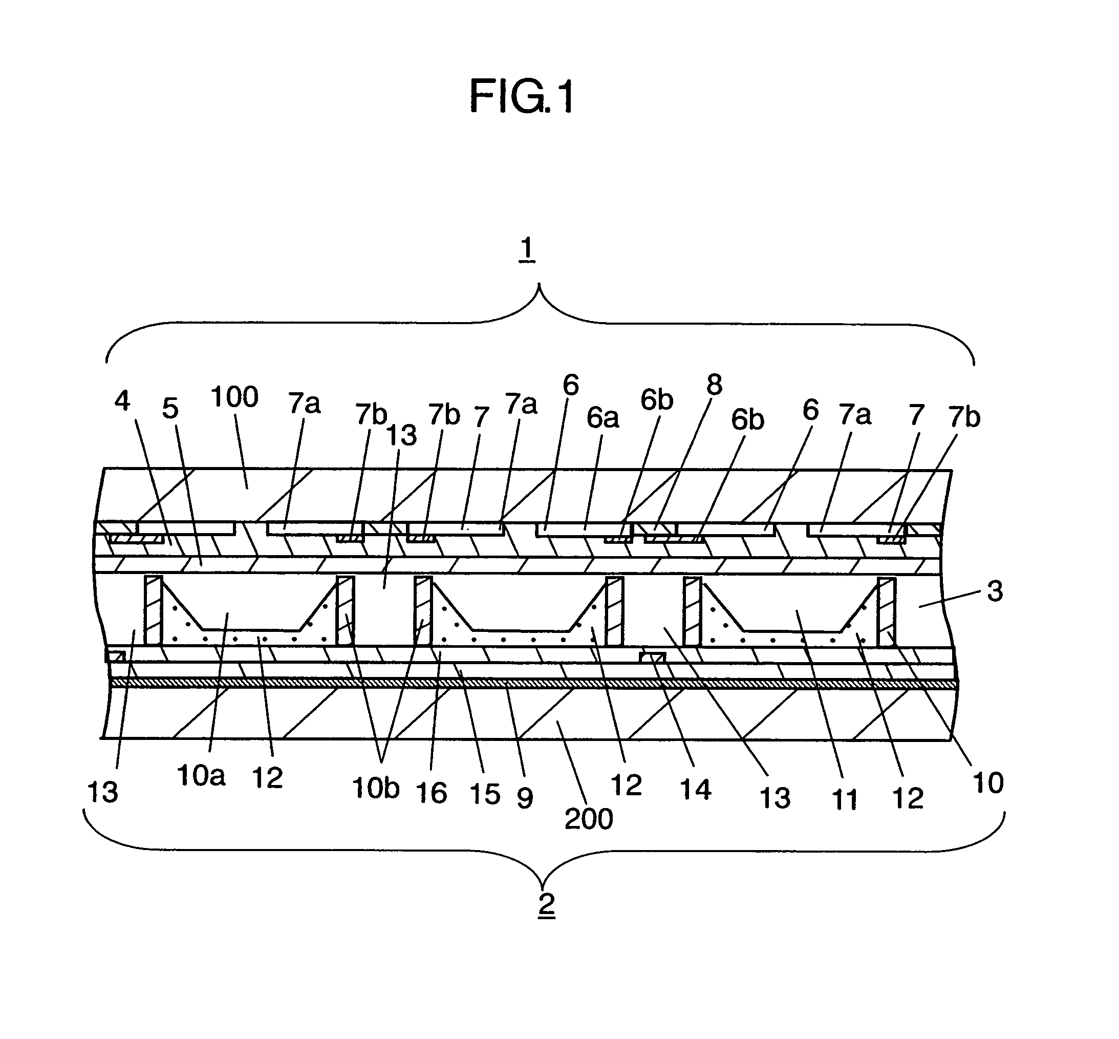
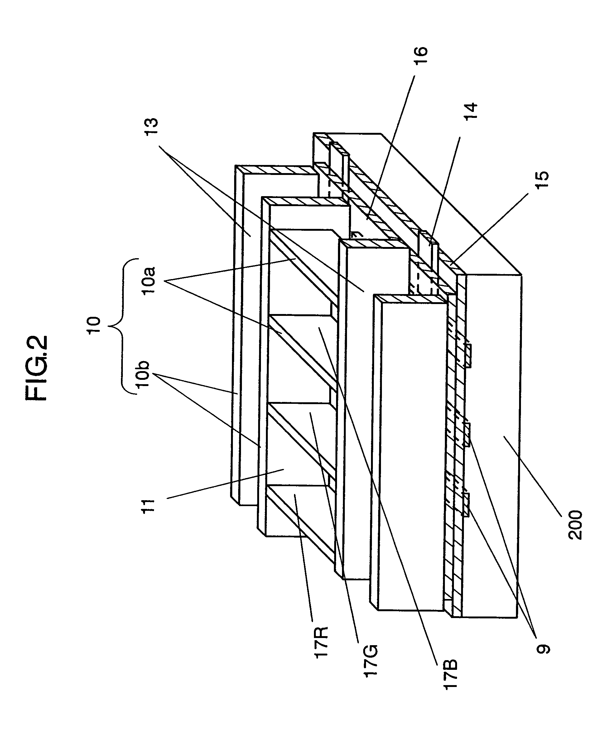
[0030]FIG. 1 shows a sectional view of a PDP in the first exemplary embodiment of the present invention. FIG. 2 is a perspective view of a rear board of the PDP in the first exemplary embodiment of the present invention.
[0031]As shown in FIG. 1, front board 1 and rear board 2 face each other with discharge space 3 in between. Gases such as neon (Ne) and xenon (Xe) are injected into this discharge space 3 and emit ultraviolet rays when subjected to electric discharge. The first electrode, which acts as a display electrode, includes stripes of a pair of scanning electrodes 6 and sustain electrodes 7 aligned in parallel and covered with dielectric layer 4 and protective film 5, and is disposed on front substrate 100. These scanning electrodes 6 and sustain electrodes 7 are configured, respectively, with transparent electrodes 6a and 7a, and metal bus lines 6b and 7b, made such as of silver (Ag) for better conductivity. Metal bus lines 6b and 7b are overlaid on transparent electrodes 6a...
second exemplary embodiment
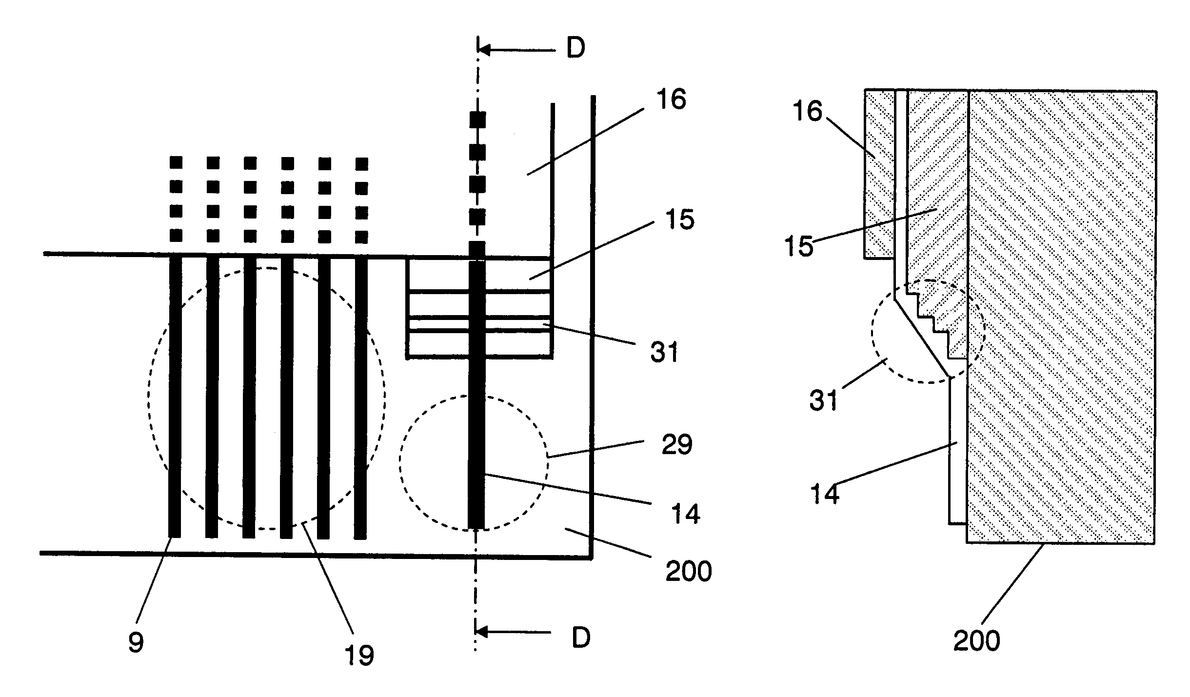
[0043]FIGS. 8A and 8B show details of a structure of a wiring lead-out of a PDP in the second exemplary embodiment of the present invention. FIG. 8A is a plan view, and FIG. 8B is a sectional view taken along D—D in FIG. 8A.
[0044]In the second exemplary embodiment, slope 31 is provided in the wiring lead-out area of priming electrode 14. In this slope 31, the film thickness of dielectric layer 15 gradually reduces in a slope toward the edge of rear substrate 200, and wiring lead-out 29 is formed on rear substrate 200. Accordingly, priming electrode 14 and data electrode 9 are in the same plane at wiring lead-out 29 connected to the FPC.
[0045]As described above, the thickness of dielectric layer 15 is gradually reduced in the wiring lead-out area of priming electrode 14 such that there is no effect of reduced thickness or line width of priming electrode 14 that is formed on dielectric layer 15. This secured the reliability of wiring of priming electrode 14. Moreover, connection to th...
third exemplary embodiment
[0047]FIGS. 9A and 9B show the details of a structure of wiring lead-out of a PDP in the third exemplary embodiment. FIG. 9A is a plan view, and FIG. 9B is a sectional view taken along E—E in FIG. 9A.
[0048]In the third exemplary embodiment, priming electrode wiring 33 formed on rear substrate 200 in advance and priming electrode 14 formed on dielectric layer 15 are connected by via hole 32 created on dielectric layer 15. This via hole is filled with conductive material. Accordingly, wiring lead-out 30 to be connected to the FPC is formed in the same plane as data electrode 9.
[0049]Via hole 32 is created such as by laser beam after forming dielectric layer 15, and the conductive material is injected into via hole 32. This method secures the wiring reliability of priming electrode 14. In addition, connection to the FPC is established in the same plane as wiring lead-out 19 of data electrode 9. This allows wiring to be carried out in the same process as connection of the FPC to data el...
PUM
 Abstract
Description
Claims
Application Information