Method of manufacturing a shielding base member

a shielding base and manufacturing method technology, applied in the field of shielding base members, can solve the problems of difficult handling of patterned metal foil, and achieve the effect of facilitating the handling of metal foil

Inactive Publication Date: 2006-08-08
KYODO INSATU KK KYODO PRINTING CO LTD
View PDF18 Cites 12 Cited by
  • Summary
  • Abstract
  • Description
  • Claims
  • Application Information

AI Technical Summary

Benefits of technology

[0039]According to the present invention, the plastic film employed as the substrate that facilitates the handling of the metal foil does not remain in the shielding base member. The near-infrared absorbing function is provided by incorporating a pi...

Problems solved by technology

As described above, since the handling of the metal foil that is patterned is not easy, the metal foil is pasted onto the plastic film via the res...

Method used


Image

  • Method of manufacturing a shielding base member
  • Method of manufacturing a shielding base member
  • Method of manufacturing a shielding base member

Examples


first embodiment

[0054]Manufacturing methods for producing the shielding base member according to the first embodiment of the present invention will first be described.

First Manufacturing Method

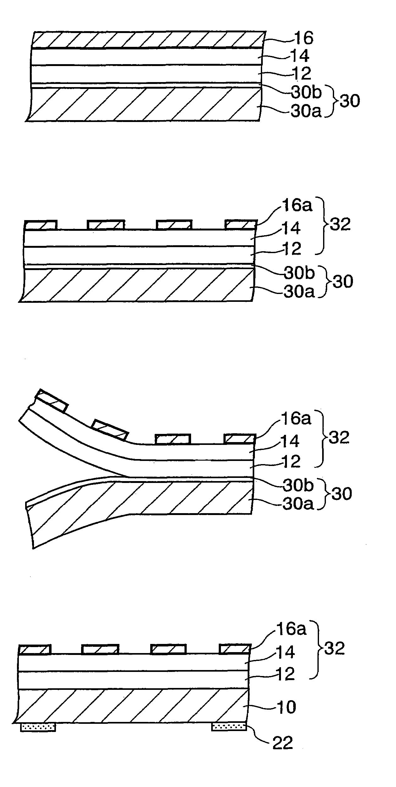
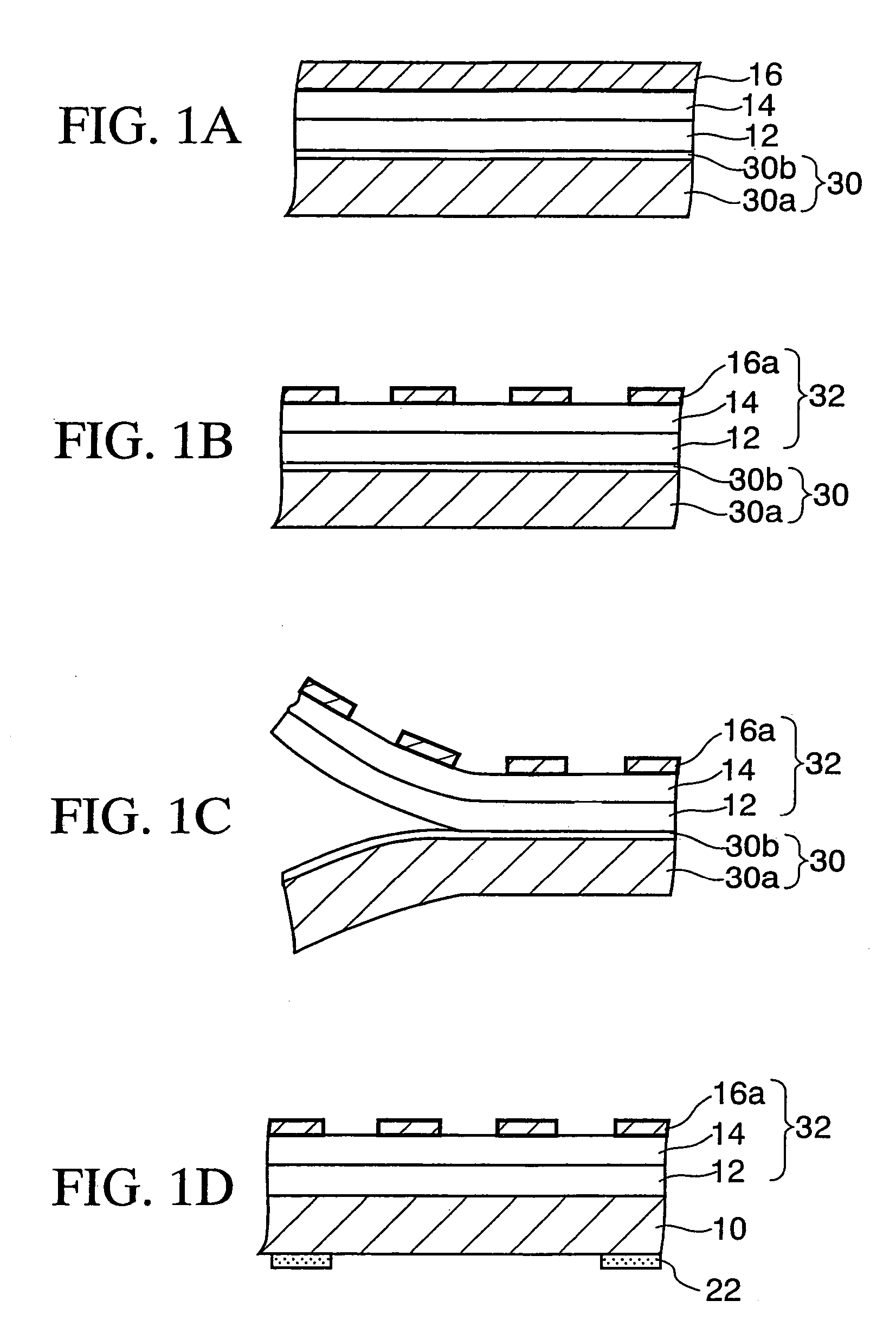
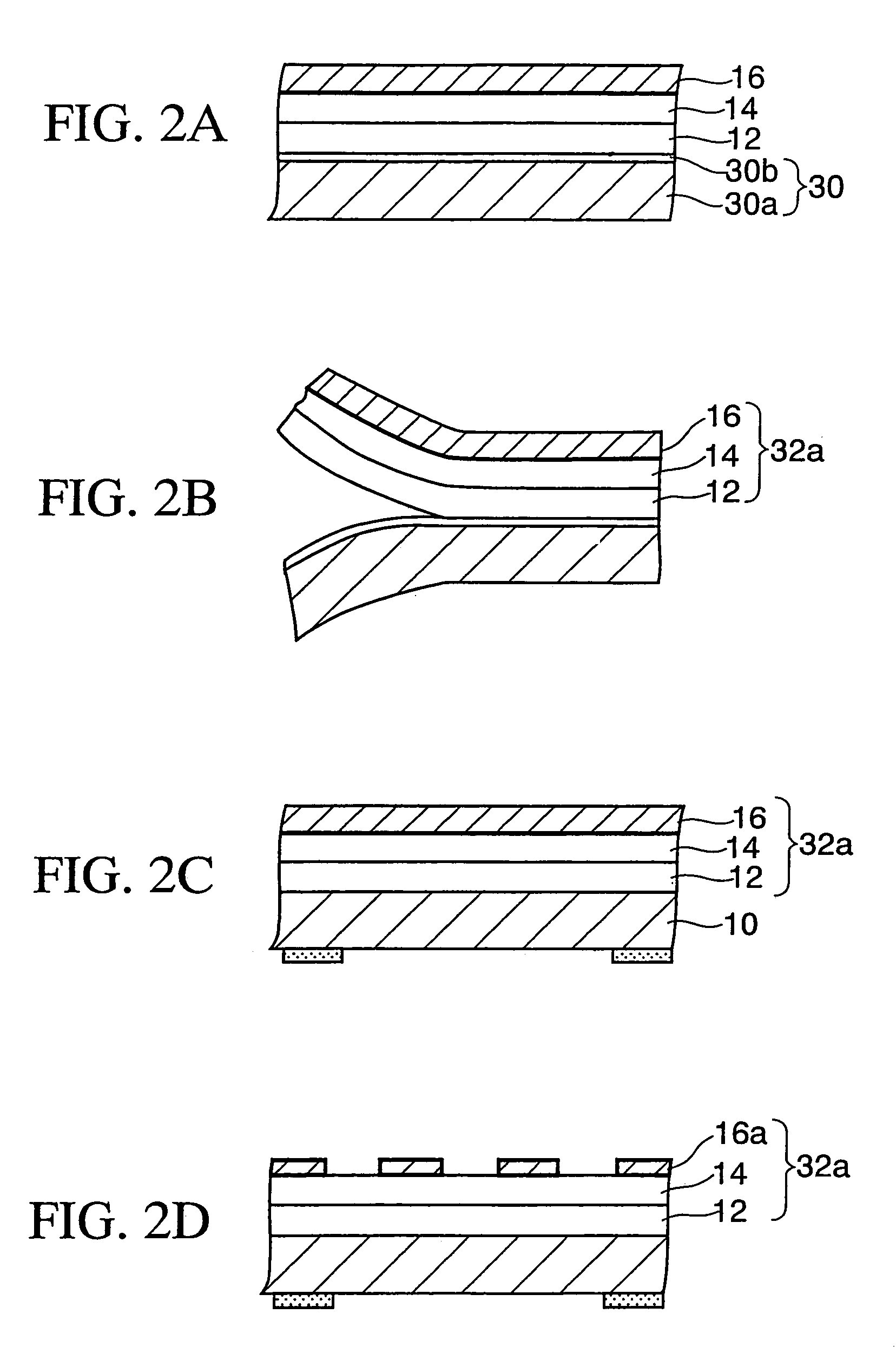
[0055]As shown in FIG. 1A, a PET (polyethylene terephthalate) film 30a is used as an example of the plastic film. A silicone layer 30b (release layer) of 1 μm, for example, is coated on one surface of this PET film 30a.

[0056]To form the silicone layer 30b a solution of 600 wt % in total is formed by mixing 100 parts by weight of the silicone (KS-3703 manufactured by Shin-Etsu Chemical Co., Ltd.), 1 part by weight of the catalyst (CAT-PL-50T), and 499 parts by weight of solvent (toluene). Then, the silicone layer 30b is formed by coating this solution on the PET film 30a by a bar coater, and then annealing at 120 ° C. for 30 seconds. This plastic film 30a on one surface of which the silicone layer 30b is formed is referred to as “separator 30” hereinafter.

[0057]Then, a first adhesive layer 12 having a thickne...

second embodiment

[0096]FIG. 4 is a schematic sectional view showing a shielding base member according to a second embodiment of the present invention. The shielding base member of the second embodiment differs from the shielding base member of the first embodiment in that it has no separate near-infrared absorbing layer and such function is given to the adhesive layer. Therefore, in FIG. 4, the same symbols are affixed to the same elements as those in FIG. 3A, and their detailed explanation will be omitted here.

[0097]As shown in FIG. 4, the shielding base member 26a of the second embodiment has a structure lacking a separate near-infrared absorbing layer. The copper layer pattern 16a is formed on the glass substrate 10 via the first adhesive layer 12 and the resin layer 14, and then the PET reflection preventing layer 20 is formed on the copper layer pattern 16a via the third adhesive layer 12b having the near-infrared absorbing function. In this manner, since the third adhesive layer 12b has the ne...

third embodiment

[0102]FIG. 5 is a schematic sectional view showing a shielding base member according to a third embodiment of the present invention. The difference between the shielding base member of the third embodiment and the shielding base member of the first embodiment is that in the third embodiment the metal layer pattern of the shielding base member is formed on the surface of the transparent substrate on the PDP side and reflection preventing layers are formed on both surfaces of the transparent substrate. Therefore, in FIG. 5, the same symbols are affixed to the same elements as those in FIG. 3A, and their detailed explanation is omitted here.

[0103]As shown in FIG. 5, in the shielding base member 26b of the third embodiment, the black frame layer 22 is formed on one surface of the glass substrate 10, i.e., the surface on the PDP side, and the copper layer pattern 16a is formed on the black frame layer 22 and the glass substrate 10 via a first adhesive layer 12c and the resin layer 14.

[01...


PUM

PropertyMeasurementUnit
Transparencyaaaaaaaaaa
Reflectionaaaaaaaaaa

Abstract

The method of forming a radiation shielding structure includes a first adhesive layer, a resin layer, and a metal foil laminated sequentially on a release layer of a plastic film. A metal layer pattern is formed from the metal foil. The first adhesive layer, the resin layer, and the metal layer pattern are formed sequentially from the bottom on a transparent substrate by separating the release layer from the first adhesive layer along an interface and then adhering the first adhesive layer to the transparent substrate.

Description

CROSS-REFERENCE TO RELATED APPLICATIONS[0001]This application is a divisional of U.S. application Ser. No. 10 / 147,905, filed May 20, 2002 now U.S. Pat. No. 6,808,773, now allowed and claims, under 35 USC 119, priority of Japanese Application No. 2001-155747 filed May 24, 2001 and Japanese Application No. 2002-54810 filed Feb. 28, 2002.BACKGROUND OF THE INVENTION[0002]1) Field of the Invention[0003]The present invention relates to a shielding base member and a method of manufacturing the same and, more particularly, a shielding base member for shielding from electromagnetic radiation, etc., that leak out from the PDP (Plasma Display Panel), etc. and a method of manufacturing the same.[0004]2) Description of the Related Art[0005]In recent-years, the applications of the PDP (Plasma Display Panel), which has a wide viewing angle and good display quality and provides a large screen, have broadened quickly into multimedia display devices, etc.[0006]The PDP is a display device that utilize...

Claims


Application Information

Patent Timeline
IPC IPC(8): H05K3/20B32B15/08H01J5/08H01J9/20H05K9/00
CPCH01J5/08H05K9/0096H01J9/20Y10T428/1481H01J2211/446H05K3/20Y10T29/49156Y10T428/1476Y10T29/49117Y10T428/1486Y10T428/1471Y10T428/24917Y10T29/49128Y10T428/14Y10T428/1438Y10T29/49124Y10T428/25Y10T428/24851Y10T29/49126B32B15/08
Inventor SHIMAMURA, MASAYOSHIOKAMOTO, RYOHEIATSUCHI, YOSHIYUKI
Owner KYODO INSATU KK KYODO PRINTING CO LTD
Why Eureka
Try Eureka