Electronic package with optimized circuitization pattern

a circuit pattern and electronic package technology, applied in the direction of printed circuit aspects, electrical apparatus construction details, printed circuit non-printed electric components association, etc., can solve the problems of high mechanical strain, flexure or bend of the organic structure by different amounts, and the interconnection between the chip carrier and the printed circuit board of the industry standard ball grid array (bga) may be subject to high stress, so as to improve the design inhibit or prevent the cracking of the circuit pattern, the effect o

Inactive Publication Date: 2006-08-08
GLOBALFOUNDRIES INC
View PDF10 Cites 4 Cited by
  • Summary
  • Abstract
  • Description
  • Claims
  • Application Information

AI Technical Summary

Benefits of technology

[0008]It is another object of this invention to provide a flexible chip carrier that provides an improved circuit pattern design on a circuitized substrate of the chip carrier.
[0009]It is yet another object of the invention to provide a flexible chip carrier that includes a circuitized substrate that will be manufactured in such a manner that substantially inhibits or prevents cracking of a circuit pattern positioned on a surface of the circuitized substrate, has increased yields and can be produced at a relatively lower costs than many current products.
[0010]It is still yet another object of the invention to provide a flexible chip carrier that substantially inhibits or prevents cracking of the circuit pattern during operation of the electronic package that results in having much improved operational field life.

Problems solved by technology

All flexible materials have some limitations on the amount of mechanical strain which can be tolerated until the material fractures and fails.
Furthermore, if the coefficient of thermal expansion (CTE) of the semiconductor chip, the chip carrier, and the printed circuit board are substantially different from one another, temperature changes during operation of the electronic package can cause flexure or bending of the organic structures by different amounts.
As a result, industry standard ball grid array (BGA) interconnections between the chip carrier and printed circuit board may be subject to high stress.
These high stresses can be transmitted into the chip carrier and can potentially cause high strain on the chip carrier materials beyond the limits of their ductility, and cause damage in the chip carrier.
Significant yield loss concerns during manufacturing, and reliability concerns during thermal cycling field operation may become manifest by failure (cracking or delamination) of dielectrics and circuitry on or within the chip carrier or even failure of the integrity of the semiconductor chip (chip cracking) caused by high stress during manufacturing and field operation.
These concerns significantly inhibit design flexibility.
These limitations may limit the electrical performance advantages of the electronic package and / or add significant cost to the electronic package.
These layers may be susceptible to stresses transmitted from the printed circuit through the BGA solder ball interconnections from handling or thermal cycling of the electronic package.
If the redistribution layer and solder mask layer cannot accommodate the stresses, then they are susceptible to deterioration, such as cracking, which can cause failure of the electronic package.
Solutions to this problem which limit or reduce the amount of printed circuit board flexure can be impractical and overly restrictive.
Yield and reliability of the chip carrier and the electronic package of which it is a part can be negatively affected.

Method used


Image

  • Electronic package with optimized circuitization pattern
  • Electronic package with optimized circuitization pattern
  • Electronic package with optimized circuitization pattern

Examples


Embodiment Construction

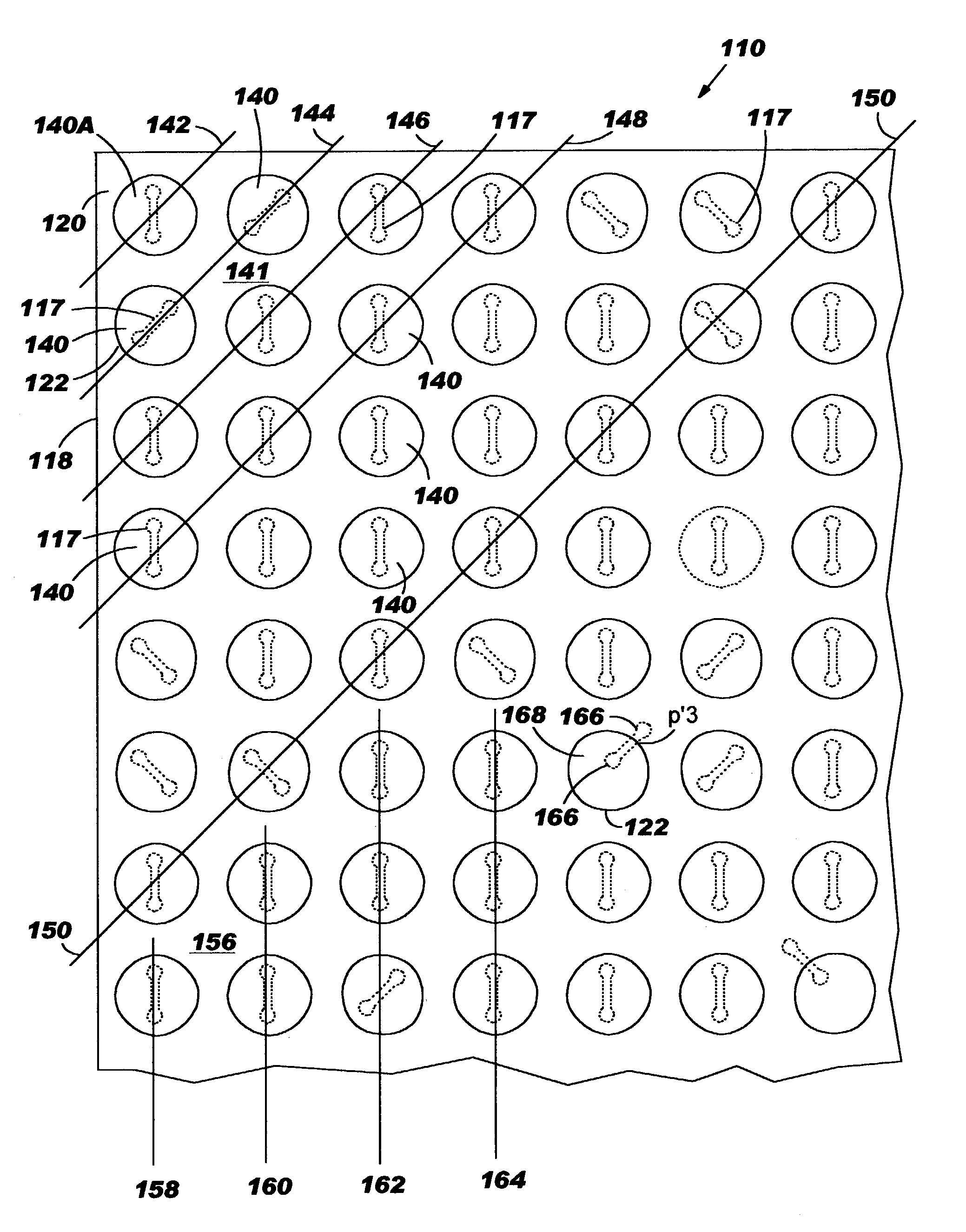
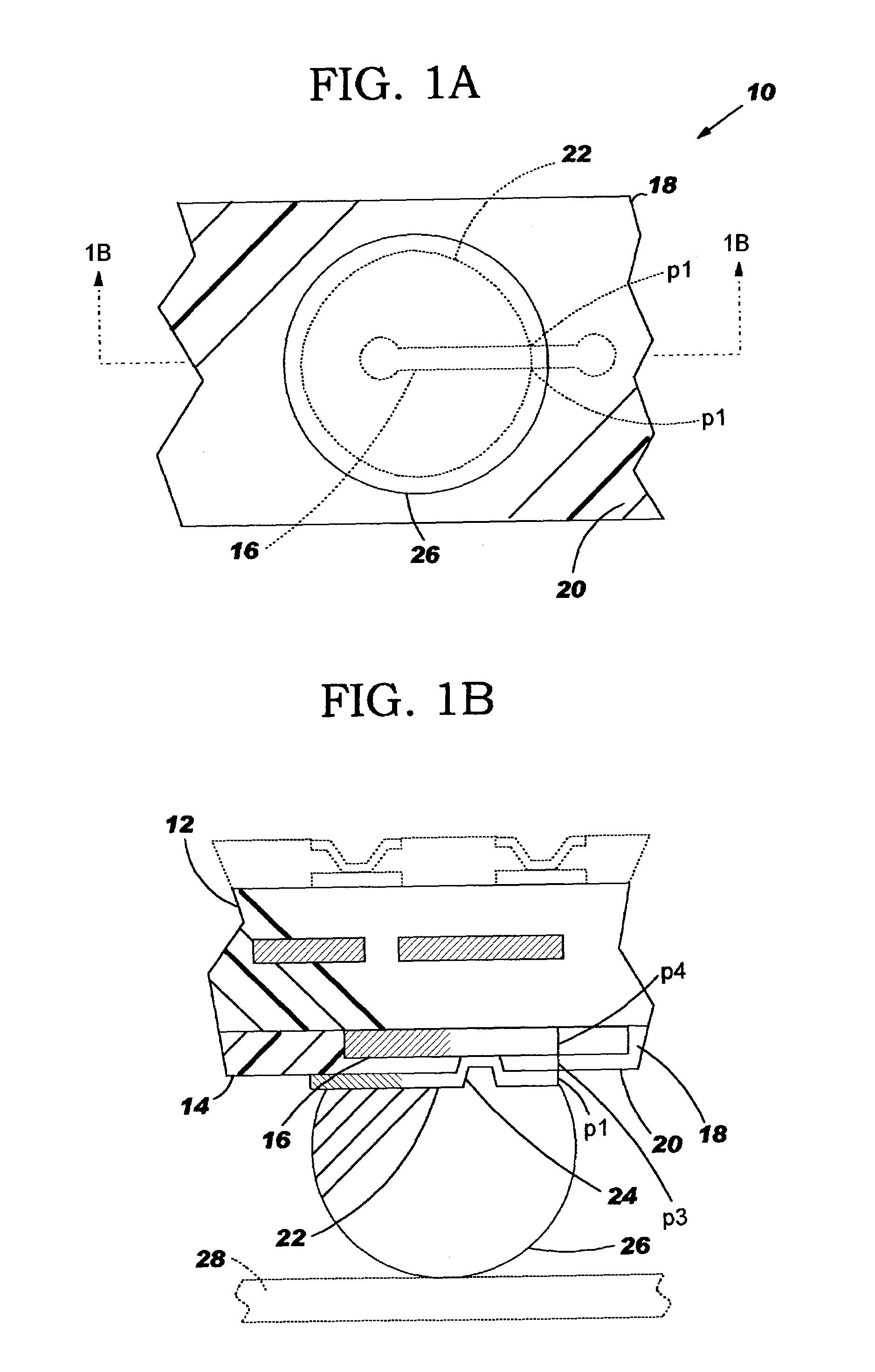
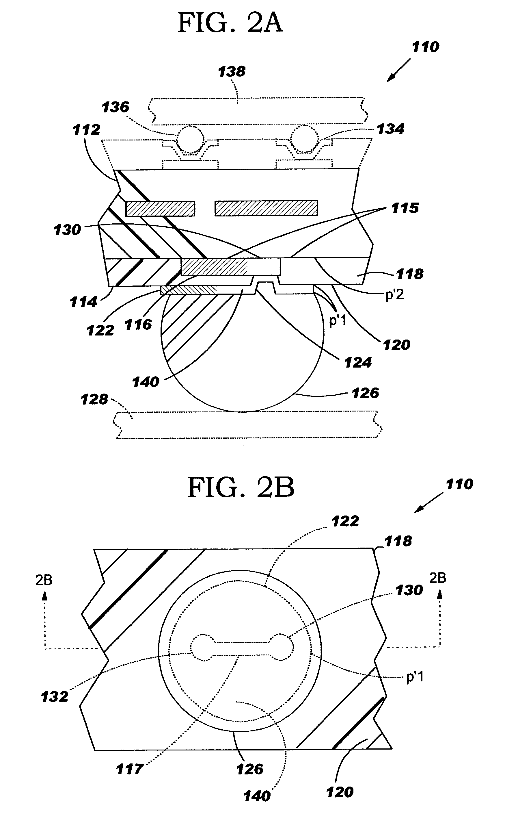
[0018]A portion of electronic package 110, for example a chip carrier, illustrating one embodiment of the present invention is shown in FIG. 2A. FIG. 2A shows a much enlarged view, in elevation, of a portion of electronic package 110 taken along line 2B—2B in FIG. 2B. FIG. 2B shows a bottom view of the portion of electronic package 110 shown in FIG. 2A. Referring to FIG. 2A, electronic package 110 includes a circuitized substrate 112 which includes a first surface 114 and a surface region 115. Surface region 115 is at a corner or a non corner edge of circuitized substrate 110. The corner surface region and non corner surface edge region will be described in greater detail below. First surface 114 has a first circuit pattern 116 thereon. An insulating layer 118 is on surface region 115 of circuitized substrate 112 and on at least a part of first circuit pattern 116. The insulating layer 118 includes an upper surface 120. A second circuit pattern 122 is electrically connected to first...


PUM

PropertyMeasurementUnit
flexibleaaaaaaaaaa
conductiveaaaaaaaaaa
areaaaaaaaaaaa

Abstract

An electronic package, such as a chip carrier, with an optimized circuit pattern having a circuitized substrate with a first and second circuit pattern is provided. The circuitized substrate includes a corner surface region. The second circuit pattern is electrically connected to the first circuit pattern on the corner surface region of the circuitized substrate and is positioned in such a manner so as to substantially inhibit cracking of the first circuit pattern during flexure of the chip carrier.

Description

FIELD OF THE INVENTION[0001]The present invention relates, in general to a flexible chip carrier for interconnecting a semiconductor chip to a printed circuit board, and in particular, to a circuitized substrate for use in such a carrier.BACKGROUND OF THE INVENTION[0002]Circuitized substrates, such as chip carriers, have been and continue to be developed for many applications. A circuitized substrate, such as an organic chip carrier for interconnecting a semiconductor chip to a printed circuit board in an electronic package, may have a surface redistribution layer for redistributing electrical signals from the circuitized substrate into a larger area so that the circuitized substrate can properly interface with the printed circuit board. A solder mask may be positioned on the redistribution layer.[0003]As semiconductor chip input / output (I / O) count increases beyond the capability of peripheral lead devices and as the need for both semiconductor chip and printed circuit board miniatu...

Claims


Application Information

Patent Timeline
Patent Type & Authority Patents(United States)
IPC IPC(8): H01L23/48H01L23/52H01L29/40H01L23/498H01L23/32H05K1/11H05K3/34H05K3/46
CPCH01L23/49811H01L23/49838H05K1/113H05K1/114H05K1/116H01L23/49822Y10T29/49149H01L2224/16225H01L2224/73253H01L2924/01078H01L2924/15312H01L2924/16195H05K1/115H05K3/3426H05K3/4602H05K2201/09454H05K2201/09472H05K2201/09509H05K2201/0979H05K2201/10318H01L2924/01019H01L2924/00014H01L2224/0401
Inventor ALCOE, DAVID J.INFANTOLINO, WILLIAMJADHAV, VIRENDRA R.
Owner GLOBALFOUNDRIES INC
Why Eureka
Try Eureka