

Frequency converter with nonlinear distortion cancellation
- Summary
- Abstract
- Description
- Claims
- Application Information
AI Technical Summary
Benefits of technology
Problems solved by technology
Method used
Image

Examples
first embodiment
(The First Embodiment)
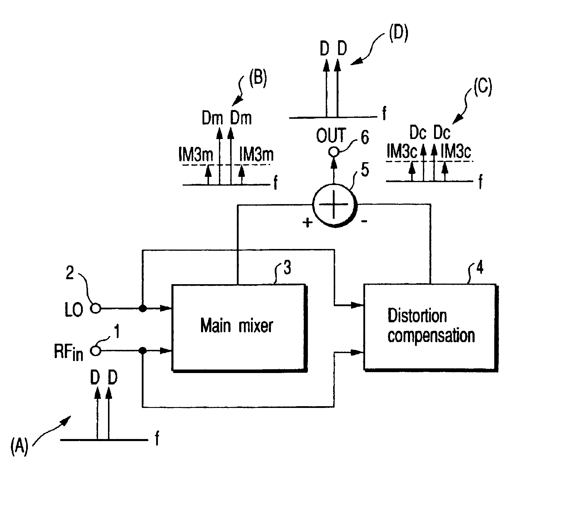
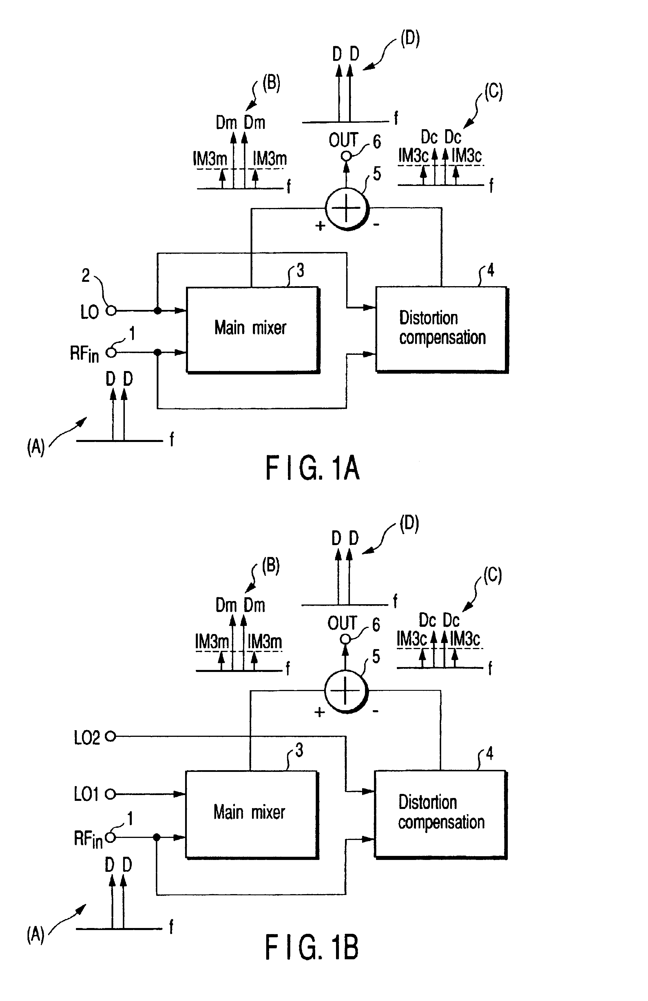
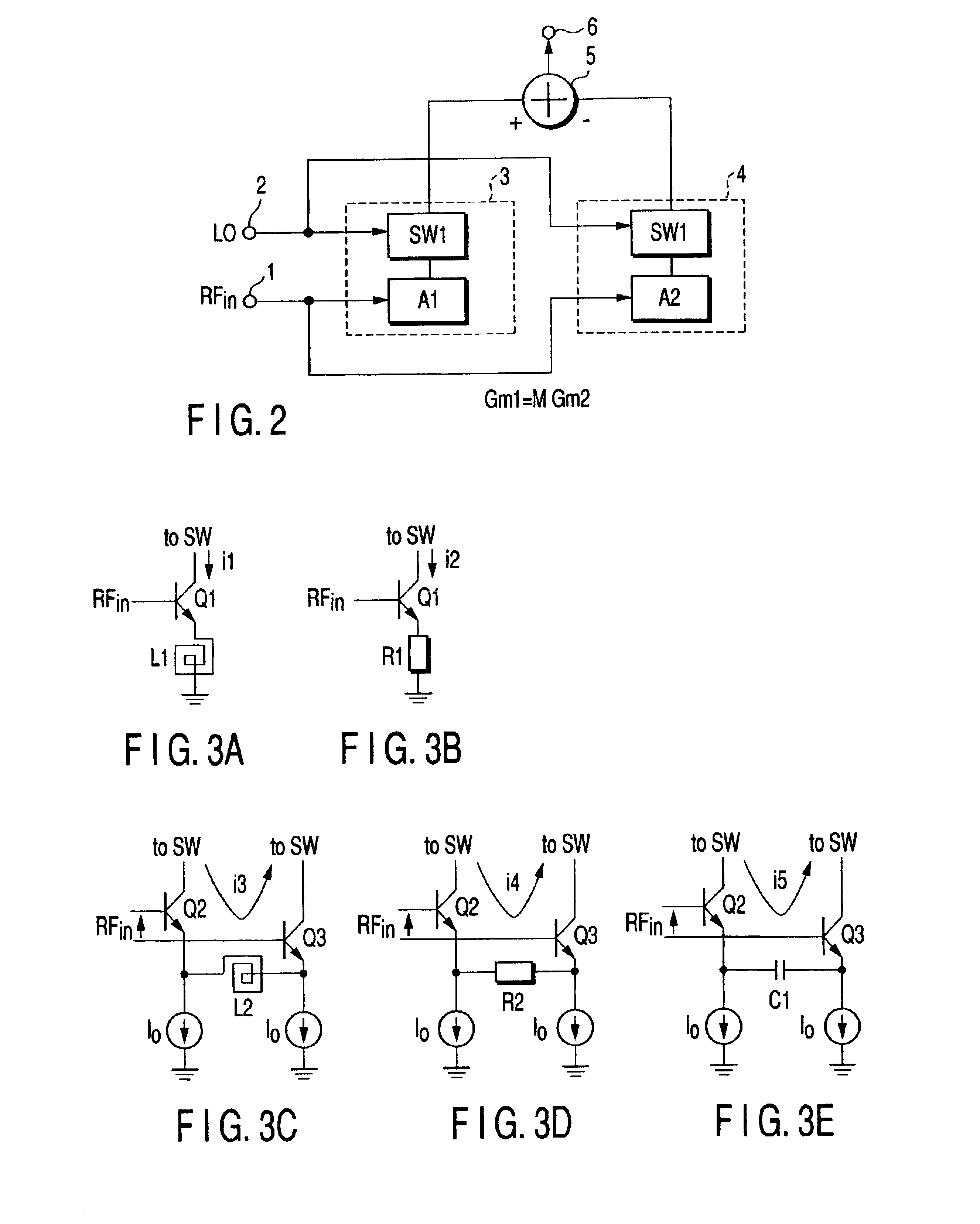
[0029]According to the frequency converter according to the first embodiment as shown in FIG. 1A, a RF input signal is input to the first input terminal 1 as an input signal to be frequency-converted, and a local signal is input to the second input terminal 2. The RF input signal and local signal are input to a main mixer (first mixer) 3, and a distortion compensation mixer (second mixer) 4. In the main mixer 3 and distortion compensation mixer 4, the RF input signal is frequency-converted according to the local signal. In other words, the main mixer 3 and distortion compensation mixer 4 function as a multiplier which multiplies the RF input signal with the local signal.
[0030]The output signals from the main mixer 3 and distortion compensation mixer 4 are added in opposite phase to each other by an adder 5. If the output signal of the main mixer 3 is a positive phase and the output signal of the distortion compensation mixer 4 is a negative phase, the output si...
second embodiment
(The Second Embodiment)
[0053]The second embodiment of the present invention will be described referring to FIGS. 5 to 8. Before describing the second embodiment concretely, there will now be described a method of selecting the emitter degeneration impedance element in the Gm amplifier in the main mixer 3 and distortion compensation mixer 4 that are explained with the first embodiment.
[0054]In the frequency converter wherein the main mixer 3 and distortion compensation mixer 4 are arranged in parallel as described in the first embodiment, it is desired for realizing low noise property that an inductance is used as the emitter degeneration impedance element in the Gm amplifier A1 in the main mixer 3. In this case, it is desired for suppressing the distortion effectively that an inductance is used as the emitter degeneration impedance element in the Gm amplifier A2 in the distortion compensation mixer 4.
[0055]Considering the frequency converter of a GHz band, the inductance used as the...
third embodiment
(The Third Embodiment)
[0064]FIG. 9 shows a frequency converter according to the third embodiment of the present invention. According to this frequency converter, the emitter degeneration impedance elements included in the Gm amplifiers A1 and A2 in the main mixer 3 and distortion compensation mixer 4 are constructed by the same kinds of elements (resistors in this embodiment), and the mixers 3 and 4 are constructed in a SBM configuration.
[0065]The main mixer 3 comprises a current switch SW1 including a differential pair of transistors Q10 and Q11, and a Gm amplifier A1 including a transistor Q14 and an emitter degeneration resistor R3. The distortion compensation mixer 4 comprises a current switch SW2 including a differential pair of transistors Q12 and Q13 and a Gm amplifier A2 including a transistor Q15 and an emitter degeneration resistor R4. The emitter terminal of the transistor Q15 is connected to a resistor R5 and a capacitor C5 via an emitter degeneration resistor R4 in seri...
PUM
 Abstract
Description
Claims
Application Information