Light emitting device and method of fabricating the same

a light emitting device and light-emitting technology, applied in the direction of semiconductor devices, basic electric elements, electrical apparatus, etc., can solve the problems of difficult use of low-refractive-index materials, achieve enhanced expression of effects, reduce total reflection, and increase light extraction efficiency

Inactive Publication Date: 2006-08-15
SHIN-ETSU HANDOTAI CO LTD
View PDF9 Cites 12 Cited by
  • Summary
  • Abstract
  • Description
  • Claims
  • Application Information

AI Technical Summary

Benefits of technology

[0012]The light extraction layer preferably has a refractive index at a dominant emission wavelength of light extracted from the active layer larger than that of the protective film of the light emission device. It is often the case that the protective film for protecting the main body of the light emitting device is formed around the light emitting device. The light extraction layer in this case is formed using an oxide having a refractive index larger than that of the protective film, in order to suppress total reflection at the interface between the light extraction layer and the protective film.
[0013]For more enhanced expression of effects of this invention, the light extraction layer preferably comprises a plurality of stacked layers which differ from each other in the refractive index, the layers being stacked so that the one disposed closer to the topmost surface side always has a smaller refractive index. A smaller difference between refractive indices of the light extraction layer and a medium composing the ambient atmosphere (air, protective film, etc.) results in a larger critical angle of total reflection on the surface of the light extraction layer, and therefore results in a larger light extraction efficiency from the light extraction layer. For the case where the light extraction layer is composed of a single species of oxide, a smaller refractive index of the oxide to be used emphasizes this tendency. Too small refractive index of the oxide semiconductor in this case, however, increases difference between refractive indices of the light emitting layer portion (cladding layer) and light extraction layer, and may raise a problem of total reflection at the interface of the both. It is therefore preferable herein to form the light extraction layer as having a plurality of layers as described in the above, so that a layer disposed more closer to the topmost surface side of the light extraction layer will always have a smaller refractive index, and this is successful in reducing difference in refractive indices at the all interfaces between the light emitting layer portion and light extraction layer, between the individual layers composing the light extraction layer, and between the light extraction layer and ambient atmosphere, and in making the total reflection less likely to occur. In other words, the light extraction layer will have a structure in which the refractive index gradually decreases towards the topmost surface in the thickness-wide direction, and formation of thus-configured light extraction layer can prevent the interface where the refractive index can extremely vary from being formed between the light emission layer portion and ambient atmosphere even if differences in the refractive indices therebetween is considerably large, and is consequently more successful in reducing a ratio of emission flux possibly returned to the light emitting layer portion due to total reflection.
[0014]It is to be noted that the refractive index may continuously be varied within the light extraction layer in the thickness-wise direction (in an exemplary case where MgxZn1-xO-type oxide is used in this structure, this is accomplished by continuously varying MgO alloy composition x in the thickness-wise direction). This is success...

Problems solved by technology

It has, however, been difficult to use these low-refractive-index materials as the light extraction layer of light emitting devices, of which light emitting layer portions are composed of conventionally-developed, oxygen-incompatible materials such as AlGaAs-base, GaAsP-base, AlGaInP-base and InGaN-ba...

Method used


Image

  • Light emitting device and method of fabricating the same
  • Light emitting device and method of fabricating the same
  • Light emitting device and method of fabricating the same

Examples


example

[0061]In this example, two types of the light emitting devices 100 having

[0062](1) no light extraction layer 7 (conventional example); and

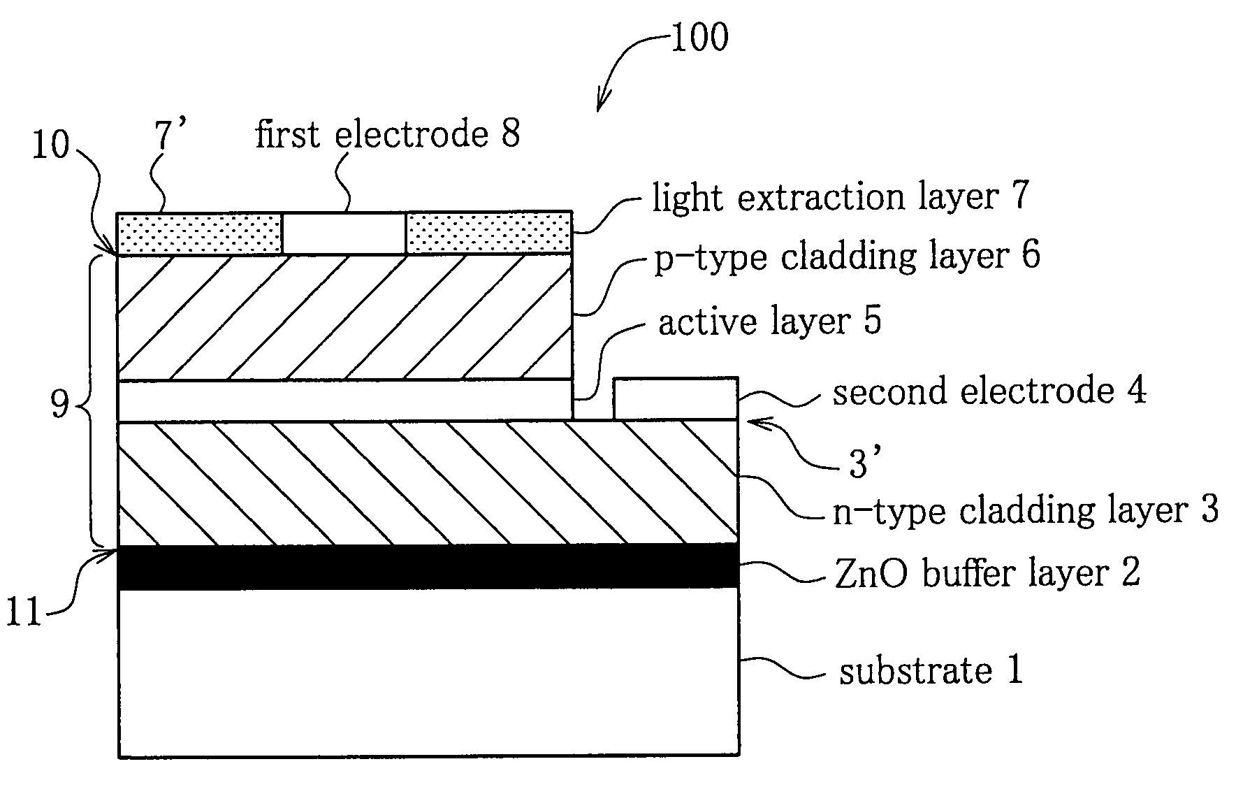
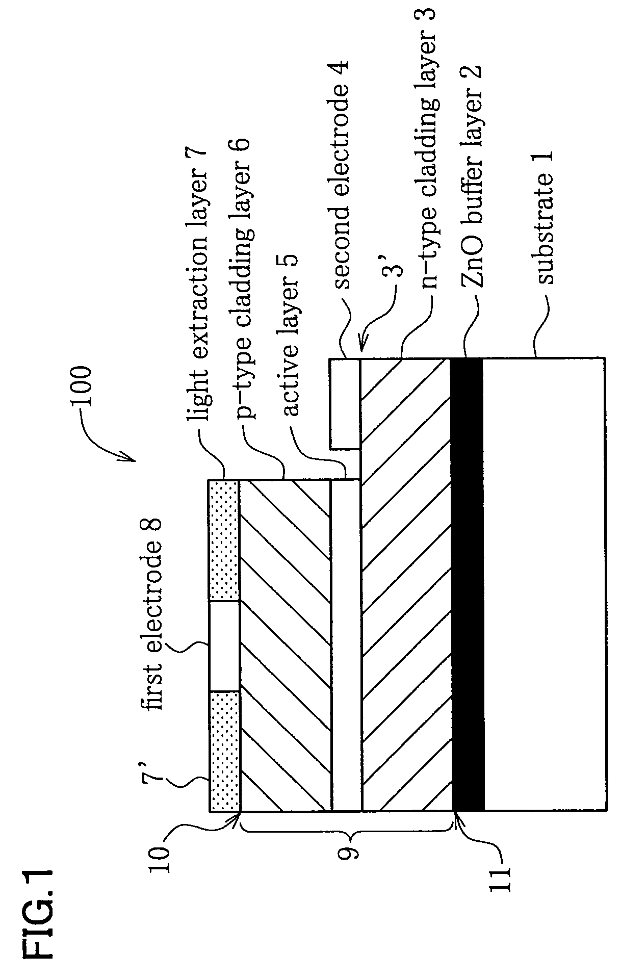
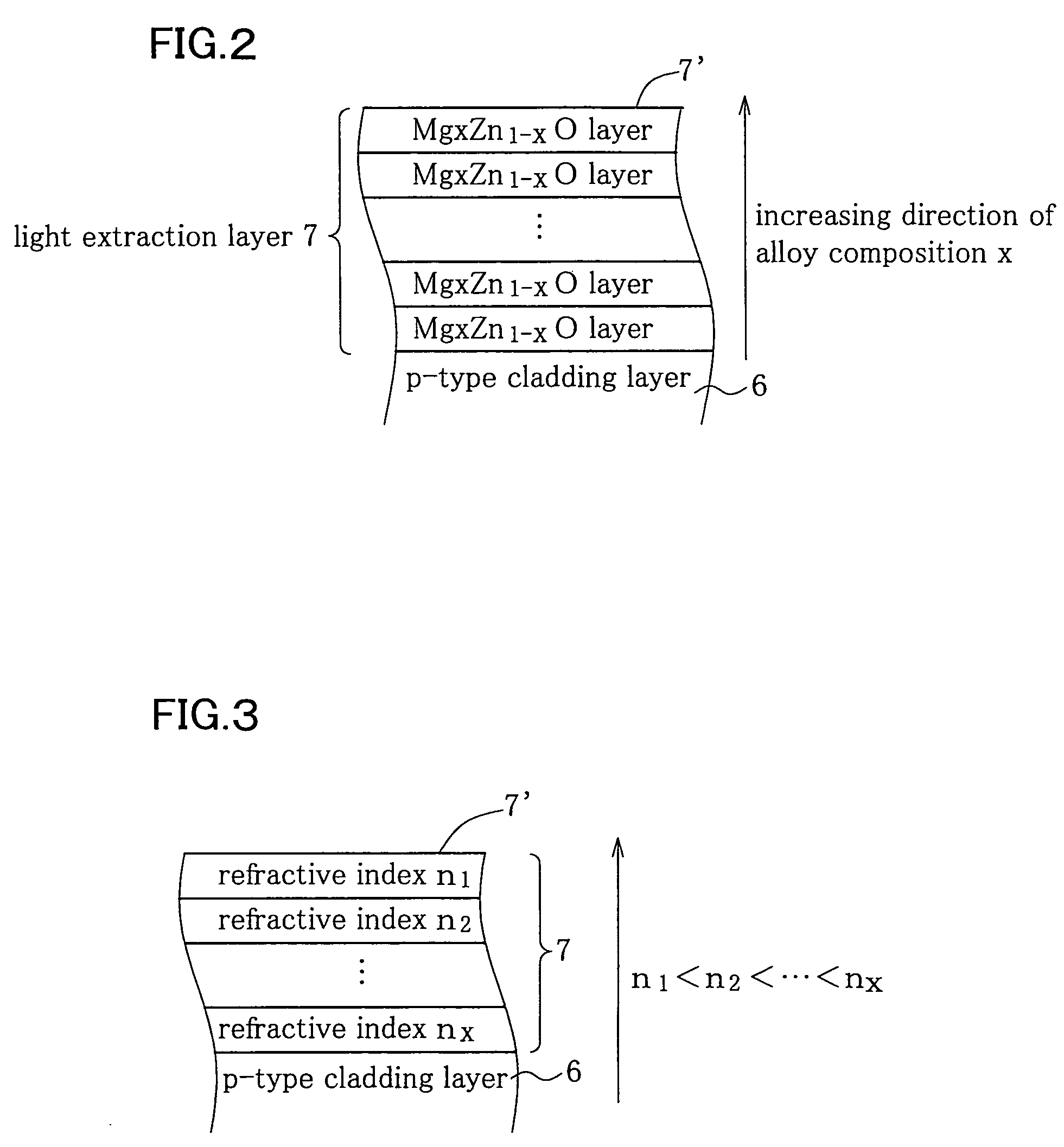
[0063](2) the light extraction layer 7 only composed of the MgO layer (refractive index: approx. 1.7); are compared for the light extraction efficiency, where each light emitting device 100 being configured, as shown in FIG. 1, as having the active layer 5 composed of zinc oxide (ZnO), the p-type cladding layer 6 composed of the MgZnO-type oxide semiconductor, and being covered by an epoxy resin as a protective film on the outer surface thereof. The resin used herein is such as having a refractive index of approximately 1.5 (e.g., epoxy resin, etc.). The light extraction layer 7 is formed on the outer side of the p-type cladding layer 6. It is to be noted that, in this example, the individual interfaces are assumed as being formed flat, and light emitted from the active layer 5 is assumed to completely follow Snell's Law. The cladding layer herein...


PUM


Abstract

A light emitting device 100 has a light emitting layer portion 9 which comprises an active layer 5 composed of an MgxZn1-xO-type oxide semiconductor, a p-type cladding layer 6 again composed of an MgxZn1-xO-type oxide semiconductor, and an n-type cladding layer 3. On the p-type cladding layer 6 of the light emitting layer portion 9, a light extraction layer 7 is configured using an oxide, where the light extraction layer 7 has a refractive index at a dominant emission wavelength of light extracted from the active layer 5 smaller than that of the cladding layers 3,6. This makes it possible to efficiently extract the light emitted from the light emitting layer portion 9 to the external of the light emitting device 100. This is it successful in providing a high-light-extraction-efficiency light emitting device having the light emitting layer portion composed of an oxide semiconductor, and a method of fabricating the same.

Description

[0001]This application is a Continuation-In-Part of PCT Application No. PCT / JP02 / 11425 filed on Nov. 1, 2002. This application also claims the priority of Japanese Patent Application No. 2001-366087 filed on Nov. 30, 2001, which is incorporated herein by reference.FIELD OF THE INVENTION[0002]This invention relates to a light emitting device and a method of fabricating the same.BACKGROUND ART[0003]To what degree light emission can occur in a light emitting layer portion, which comprises an active layer and cladding layers, is an important index for performances of light emitting devices such as light emitting diode and semiconductor laser. An exemplary configuration popularly adopted is double heterostructure, in which the cladding layers and so forth, which function as confining and injecting carriers, are designed to be transparent to the light emission from the active layer (designed to have a band gap energy wider than a photon energy corresponded to the emission wavelength), and...

Claims


Application Information

Patent Timeline
IPC IPC(8): H01L33/00H01L33/12H01L33/28
CPCH01L33/44H01L33/28
Inventor ISHIZAKI, JUN-YA
Owner SHIN-ETSU HANDOTAI CO LTD
Why Eureka
Try Eureka