Image display device and method of manufacturing the same
a technology of image display and display device, which is applied in the manufacture of electric discharge tubes/lamps, vacuum obtaining/maintenance, tubes with screens, etc., can solve the problems of destroying the whole display device, affecting the electron source, and deteriorating the electron source, so as to achieve less deterioration and less luminance.
- Summary
- Abstract
- Description
- Claims
- Application Information
AI Technical Summary
Benefits of technology
Problems solved by technology
Method used
Image

Examples
embodiment 1
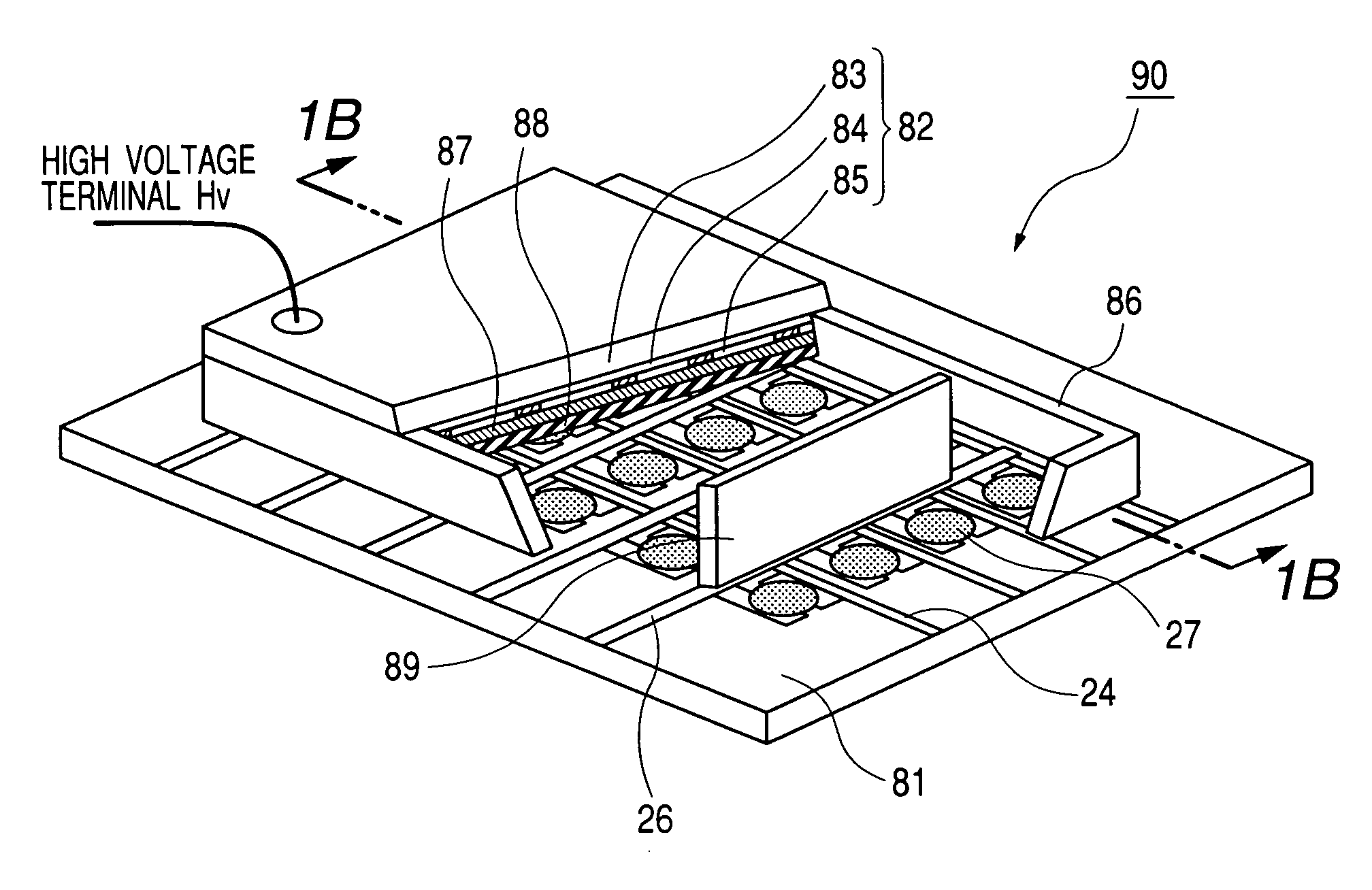
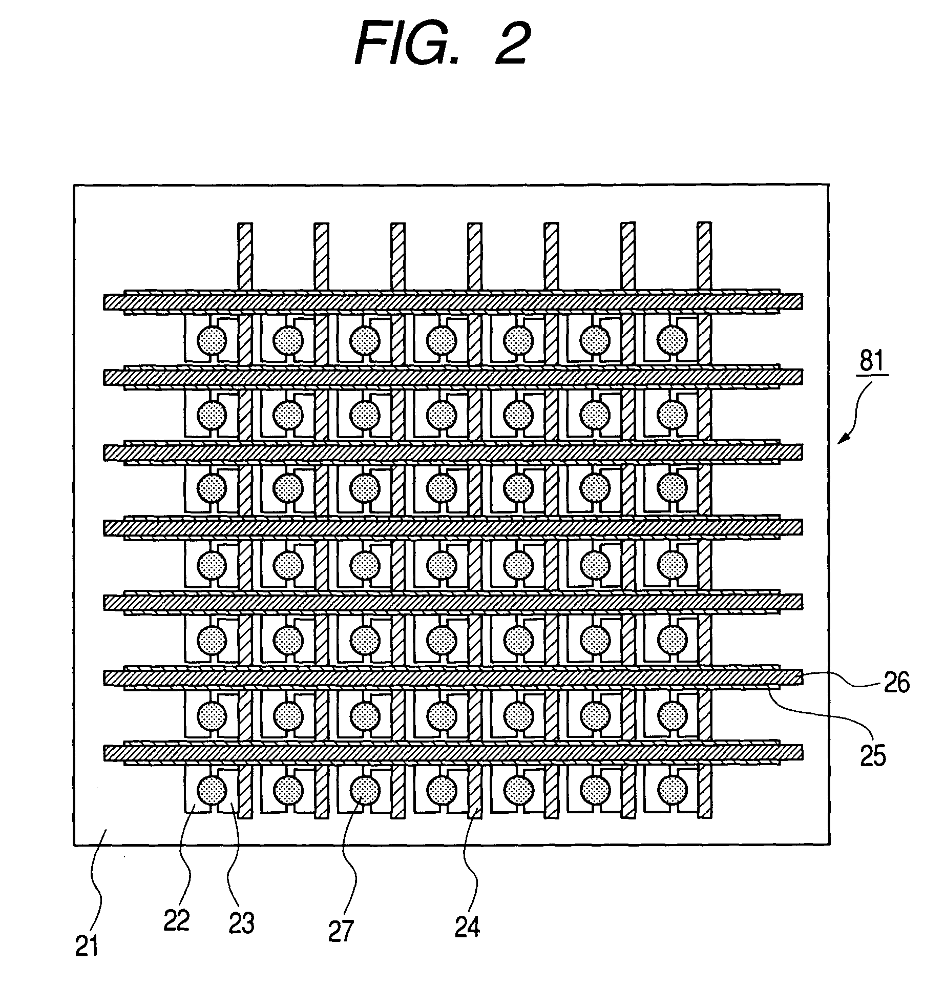
[0172]This embodiment describes an example of manufacturing an image display device as the one shown in FIGS. 1A and 1B from an electron source substrate as the one shown in FIG. 2 which has a large number of surface conduction electron-emitting devices connected in accordance with matrix wiring.
[0173]First, an electron source substrate manufacturing method according to this embodiment is described with reference to FIGS. 2, 3, 4, 5, 6, 7A, 7B and 7C.
(Formation of Device Electrodes)
[0174]This embodiment uses as the material of a substrate 21 electric glass for plasma displays which is reduced in alkaline content, specifically, PD-200, a product of Asahi Glass Co., Ltd. On the glass substrate 21, a titanium (Ti) film with a thickness of 5 nm is formed first by sputtering and then a platinum (Pt) film with a thickness of 40 nm, thereby obtaining an underlayer. Then photo resist is applied, followed by a series of photolithography processes including exposure to light, development, and...
embodiment 2
[0212]This embodiment describes an example of manufacturing an image display device as the one shown in FIGS. 13A and 13B from an electron source substrate as the one shown in FIG. 2 which has a large number of surface conduction electron-emitting devices connected in accordance with matrix wiring.
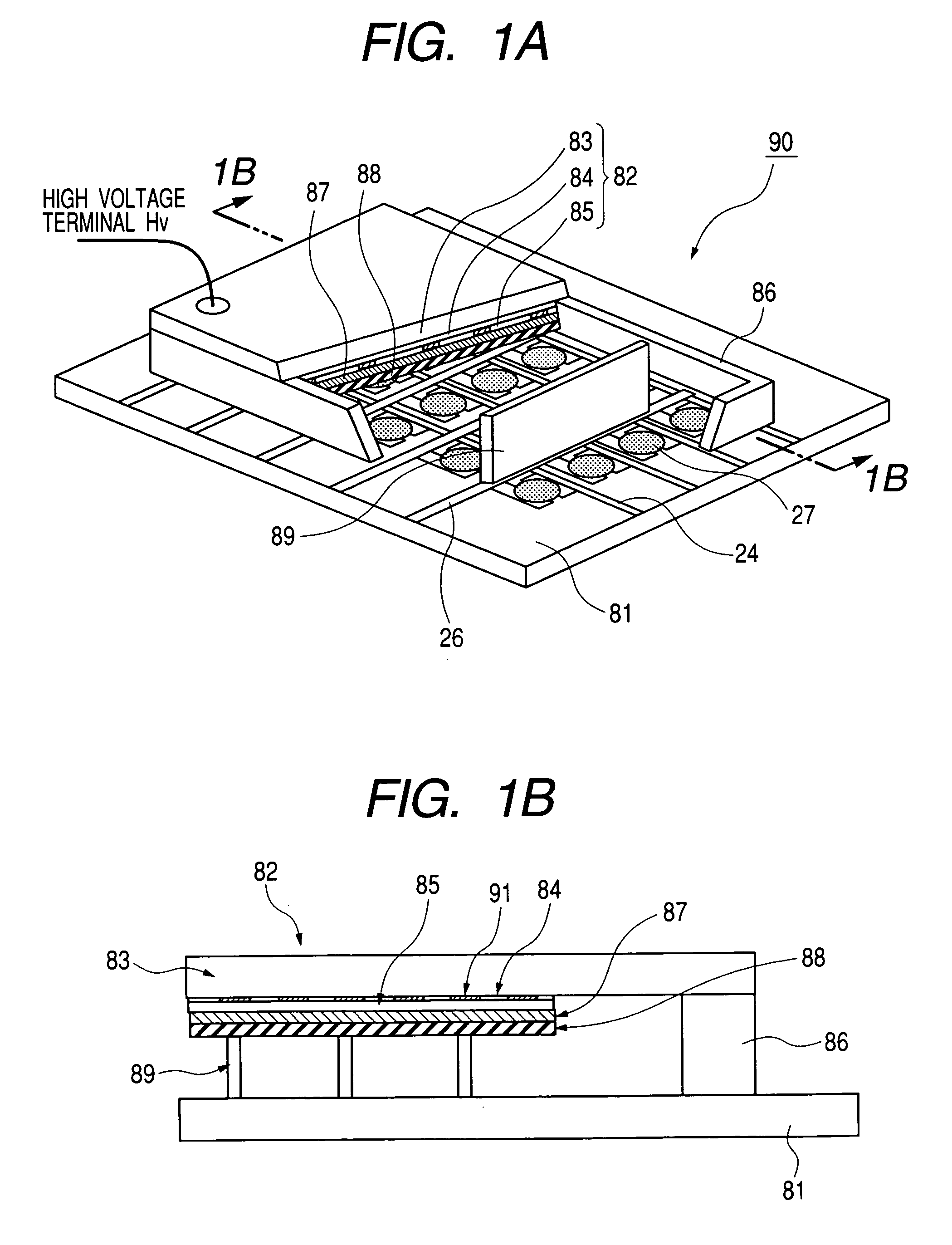
[0213]FIG. 13A is an overall perspective view schematically showing an image display device. In FIG. 13A, a supporting frame 86 and a face plate 82 are partially cut off in order to illustrate the internal structure of an airtight container 90. FIG. 13B is a partial sectional view taken along the line 1B—1B in FIG. 13A. In FIGS. 13A and 13B, components identical to those in FIGS. 1A and 1B are denoted by the same symbols.
[0214]Unlike Embodiment 1 where an additional thin film Ti getter is formed on the black conductors 91 alone, this embodiment places an additional non-evaporating getter 87 also on the X direction wirings 26 of the electron source substrate 81.
[0215]Formation of the non-ev...
embodiment 3
[0218]In this embodiment, steps from a device electrode formation step through a bonding member placement step are identical with those in Embodiment 1.
(Set Step)
[0219]Next, the electron source substrate 81 to which the supporting frame 86 is fixed and the face plate 82 are set under a vacuum atmosphere as shown in FIG. 11.
(Formation of a Non-Evaporating Getter)
[0220]On the metal back 85 of the face plate 82, Ti is deposited by RF sputtering to obtain a 500 Å thick Ti film as a non-evaporating getter 87 (See FIG. 16A). The deposition uses a metal mask that has a large opening at the center, so that the non-evaporating getter 87 is formed only within the image display region.
(Baking Step)
[0221]The face plate 82 and the electron source substrate 81 are held at a fixed distance from each other as shown in FIG. 11 and, in this state, subjected to vacuum heating. The temperature in the substrate vacuum baking is set to 300° C. or higher, so that the substrates release gas, the non-evapor...
PUM
 Abstract
Description
Claims
Application Information
 - R&D
- Intellectual Property
- Life Sciences
- Materials
- Tech Scout
- Unparalleled Data Quality
- Higher Quality Content
- 60% Fewer Hallucinations
Browse by: Latest US Patents, China's latest patents, Technical Efficacy Thesaurus, Application Domain, Technology Topic, Popular Technical Reports.
© 2025 PatSnap. All rights reserved.Legal|Privacy policy|Modern Slavery Act Transparency Statement|Sitemap|About US| Contact US: help@patsnap.com