Method and system for classifying an integrated circuit for optical proximity correction

Inactive Publication Date: 2006-08-15
BELL SEMICON LLC
View PDF19 Cites 219 Cited by
  • Summary
  • Abstract
  • Description
  • Claims
  • Application Information

AI Technical Summary

Benefits of technology

[0013]By identifying and grouping congruent local task regions in the IC chip, according to the method and system disclosed herein, only one OPC procedure (e.g., evaluation and correction) needs to be performed per group of congruent local task reg

Problems solved by technology

Commensurate with this size reduction, various process limitations have made IC fabrication more difficult.
This causes the projected image to exhibit some rounding and other optical distortion.
While such effects pose relatively little difficulty in layouts with large feature sizes (e.g., layouts with critical dimensions above about 1 micron), they cannot be ignored in layouts having features smaller than about 1 micron.
The problems become especially pronounced in IC designs having feature sizes near the wavelength of light used in the photolithographic process.
A p

Method used


Image

  • Method and system for classifying an integrated circuit for optical proximity correction
  • Method and system for classifying an integrated circuit for optical proximity correction
  • Method and system for classifying an integrated circuit for optical proximity correction

Examples


Embodiment Construction

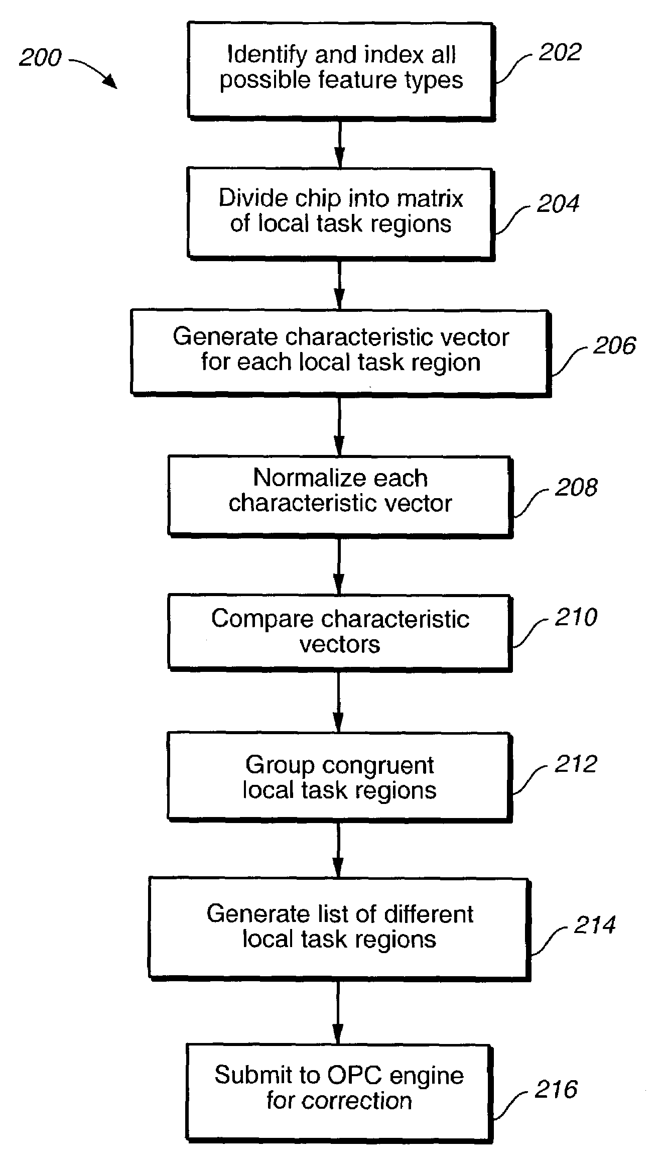
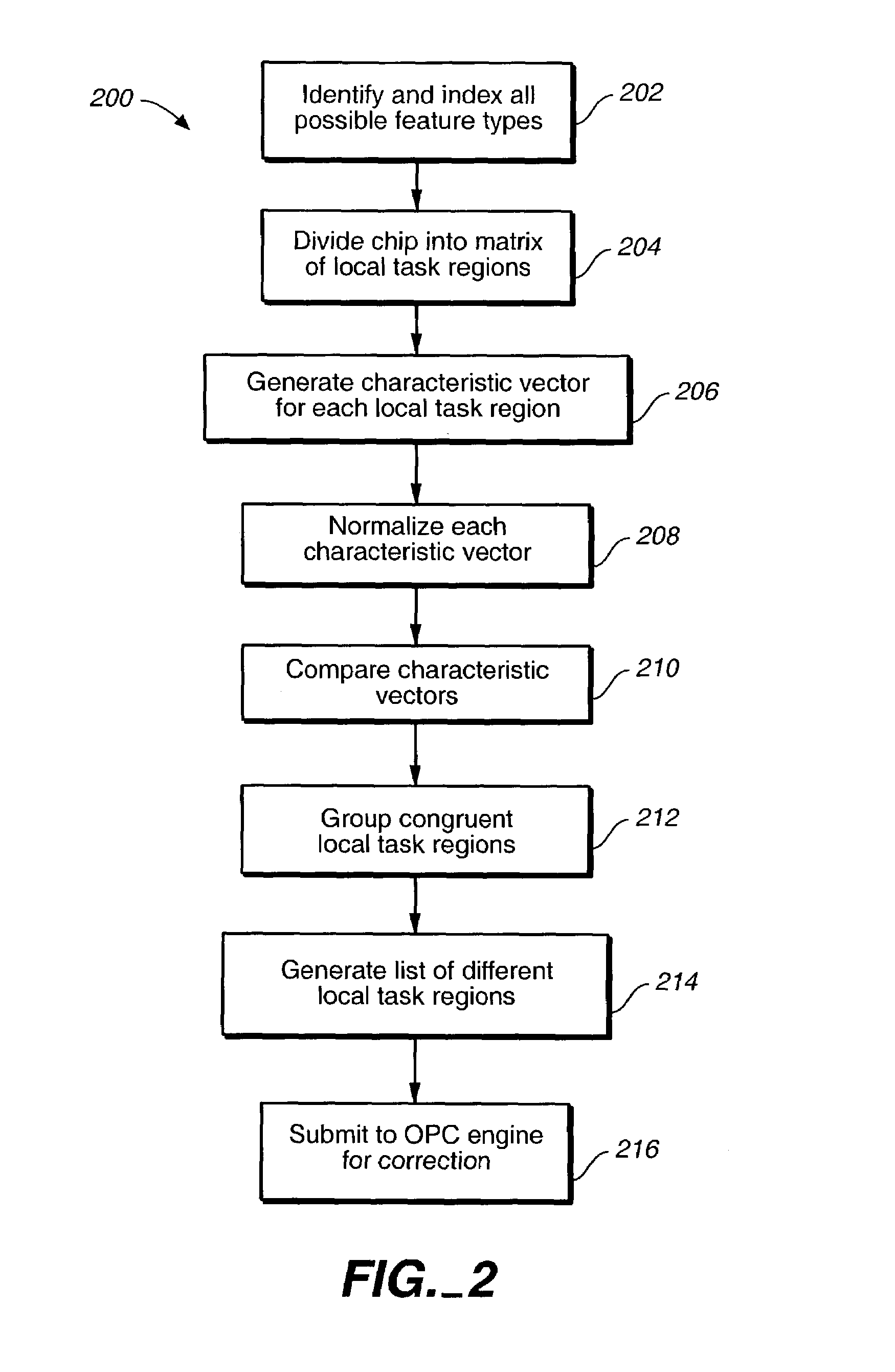
[0023]The present invention relates to a method and system for performing OPC on an IC chip design. The following description is presented to enable one of ordinary skill in the art to make and use the invention and is provided in the context of a patent application and its requirements. Various modifications to the preferred embodiments and the generic principles and features described herein will be readily apparent to those skilled in the art. Thus, the present invention is not intended to be limited to the embodiment shown but is to be accorded the widest scope consistent with the principles and features described herein.

[0024]As discussed above, OPC is a technique that corrects a mask design for potential light diffraction effects. In conventional systems, a mask design is fully created and is then corrected using an OPC technique. Some examples of OPC techniques are described in Otto, et al., Automate Optical Proximity Correction-A Rules-based Approach, SPIE Optical / Laser Micr...


PUM


Abstract

A method and system for performing optical proximity correction (OPC) on an integrated circuit (IC) chip design is disclosed. The system and method of the present invention includes dividing the IC chip into a plurality of local task regions, identifying congruent local task regions, classifying congruent local task regions into corresponding groups, and performing OPC for each group of congruent local task regions.
By identifying and grouping congruent local task regions in the IC chip, according to the method and system disclosed herein, only one OPC procedure (e.g., evaluation and correction) needs to be performed per group of congruent local task regions. The amount of data to be evaluated and the number of corrections performed is greatly reduced because OPC is not performed on repetitive portions of the IC chip design, thereby resulting in significant savings in computing resources and time.

Description

CROSS REFERENCE TO RELATED APPLICATION[0001]This application is related to patent application Ser. No. 10 / 327,314 (now is U.S. Pat. No. 6,898,780) entitled “Method and System for Constnacting A Hierarchy-Driven Chip Covering for Optical Proximity Correction,” filed on the same day and assigned to the same Assignee as the present application.FIELD OF THE INVENTION[0002]The present invention relates to integrated circuit chip design, and more particularly to performing optical proximity correction on an integrated circuit design.BACKGROUND OF THE INVENTION[0003]The minimum feature sizes of integrated circuits (ICs) have been shrinking for years. Commensurate with this size reduction, various process limitations have made IC fabrication more difficult. One area of fabrication technology in which such limitations have appeared is photolithography.[0004]Photolithography involves selectively exposing regions of a resist coated silicon wafer to a radiation pattern, and then developing the ...

Claims


Application Information

Patent Timeline
IPC IPC(8): G06F17/50G03F1/00G03F1/36G03F7/20
CPCG03F1/144G03F7/70441G03F1/36
Inventor ANDREEV, ALEXANDREPAVISIC, IVANIVANOVIC, LAV
Owner BELL SEMICON LLC
Why Eureka
Try Eureka