Antireflective member and electronic equipment using same

a technology of anti-reflective elements and electronic equipment, applied in the field of anti-reflective elements, can solve the problems of reducing yield, increasing costs, and difficult to obtain the anti-reflective effect of light having a wavelength range, and achieve the effect of stable spectral characteristics

Inactive Publication Date: 2006-08-22
SANYO ELECTRIC CO LTD
View PDF8 Cites 53 Cited by
  • Summary
  • Abstract
  • Description
  • Claims
  • Application Information

AI Technical Summary

Benefits of technology

[0021]According to the above structure, stable spectral characteristics can be obtained by forming the antireflective pattern on the surface of the substrate in the molding process of the substrate. Besides, the antireflective member can obtain spectral characteristics with low reflectance over visible light range by forming with the transfer rate from the mold not less than 70% and setting the aspect ratio of the protrusion, which is in a continuous pattern of a fine pyramidal shape or a fine conical shape and formed in the mold, not less than 1.

Problems solved by technology

In the above method to form the antireflective film consisting of the dielectric thin films on the surface of the optical element, however, it is difficult to obtain the antireflective effect for light having a wavelength range if the antireflective film is made with a few dielectric thin films.
A vacuum evaporation method to form the dielectric thin films causes variation of thickness of the films, resulting in instability of performance.
In addition, after molding a substrate to be an optical element in one process, the method needs another process to form the dielectric thin film on the surface of the substrate, thereby reducing yields and increasing costs.
Due to this, a refraction index of materials and a thickness of each dielectric thin film need to be controlled with high accuracy in the process of producing the dielectric thin film, thereby increasing costs with an increase in number of the dielectric thin film to be deposited.
In addition, the increase in number of the dielectric thin film causes warps or the like in the substrate of the optical element, thereby reducing yields.
Besides, limitations in materials of the film make it difficult to obtain ideal spectral characteristics.
In a structure disclosed in JP 88001 / 1993A, however, it is difficult in principle to form pyramidal shapes with the aspect ratio of not less than one.
Also in a structure disclosed in JP 96902 / 1987A, there is a possibility that incident light is reflected diffusely because of irregular shapes of the protrusions, resulting in low efficiency.
Although a surface treatment method of which the spindle shape with a large aspect ratio is formed on the optical element is proposed in JP 272505 / 2001A, the process, forming the metallic mask of chromium (Cr), aluminum (Al) or the like on the optical element and subjecting the optical element to reactive ion etching until the metallic mask vanishes, becomes complicated with increase in cost.

Method used


Image

  • Antireflective member and electronic equipment using same
  • Antireflective member and electronic equipment using same
  • Antireflective member and electronic equipment using same

Examples


Embodiment Construction

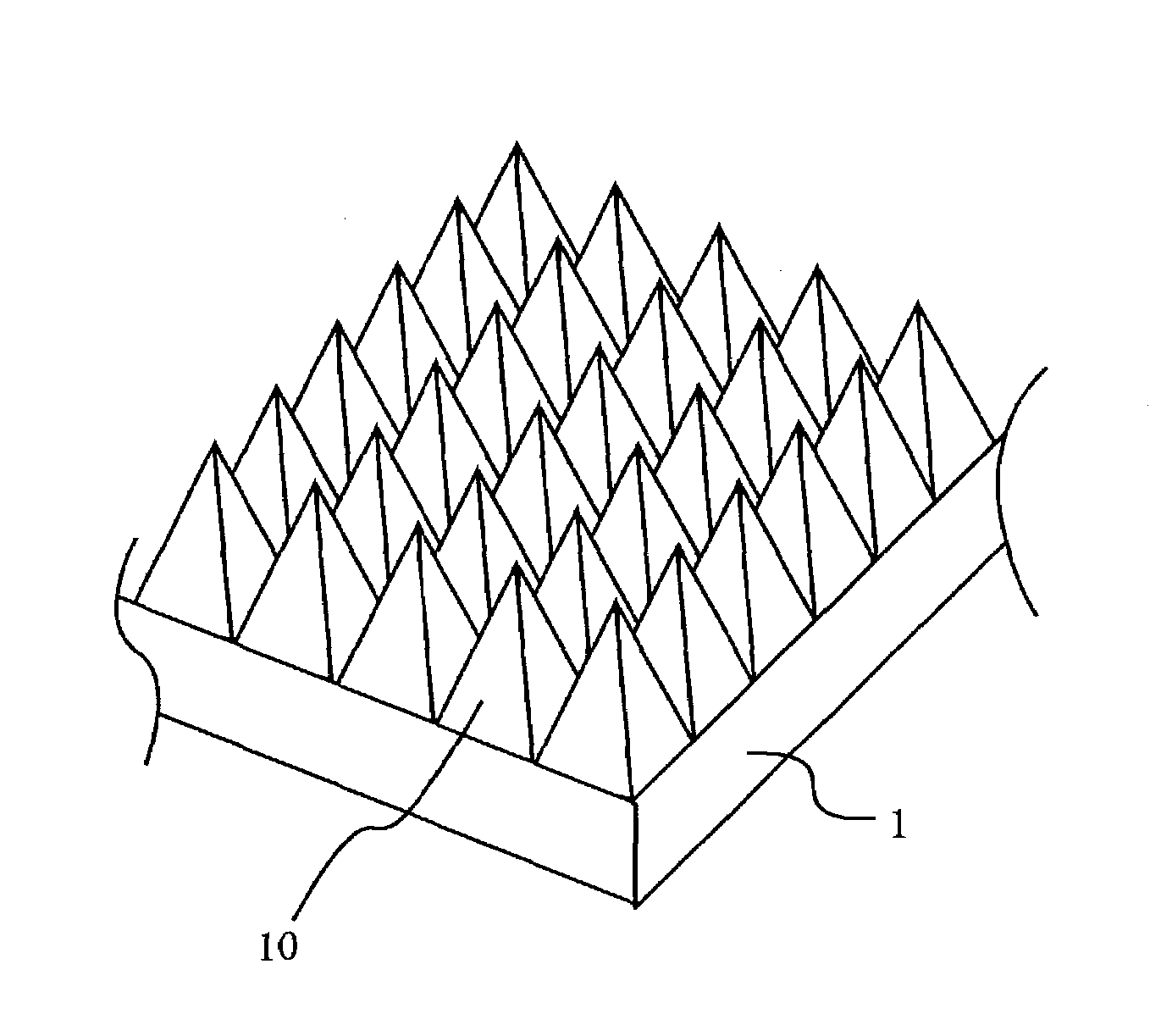
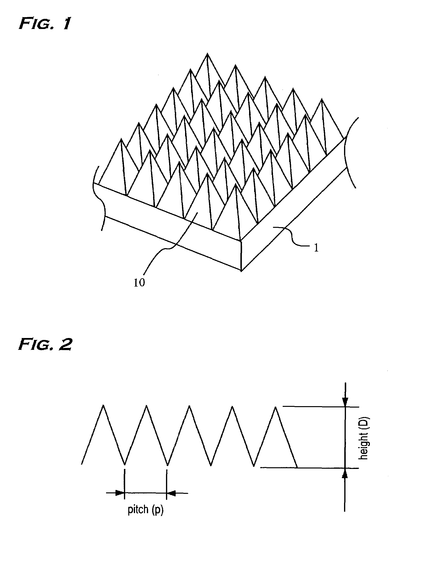
[0046]Description of an embodiment according to the present invention is now made with reference to drawings. FIG. 1 is a perspective view showing a simplified shape of a surface of an antireflective member using this invention. FIG. 2 is a schematic view showing a cross-sectional shape of the pattern.

[0047]As shown in FIG. 1, a transparent substrate 1 comprises a roughened surface having a continuous pattern in which protrusions 10 in a fine pyramidal shape are continuously formed. Although the protrusion 10 takes the shape of pyramid in this embodiment, the present invention may employ protrusions in the shape of six-sided pyramid or in the shape of cone.

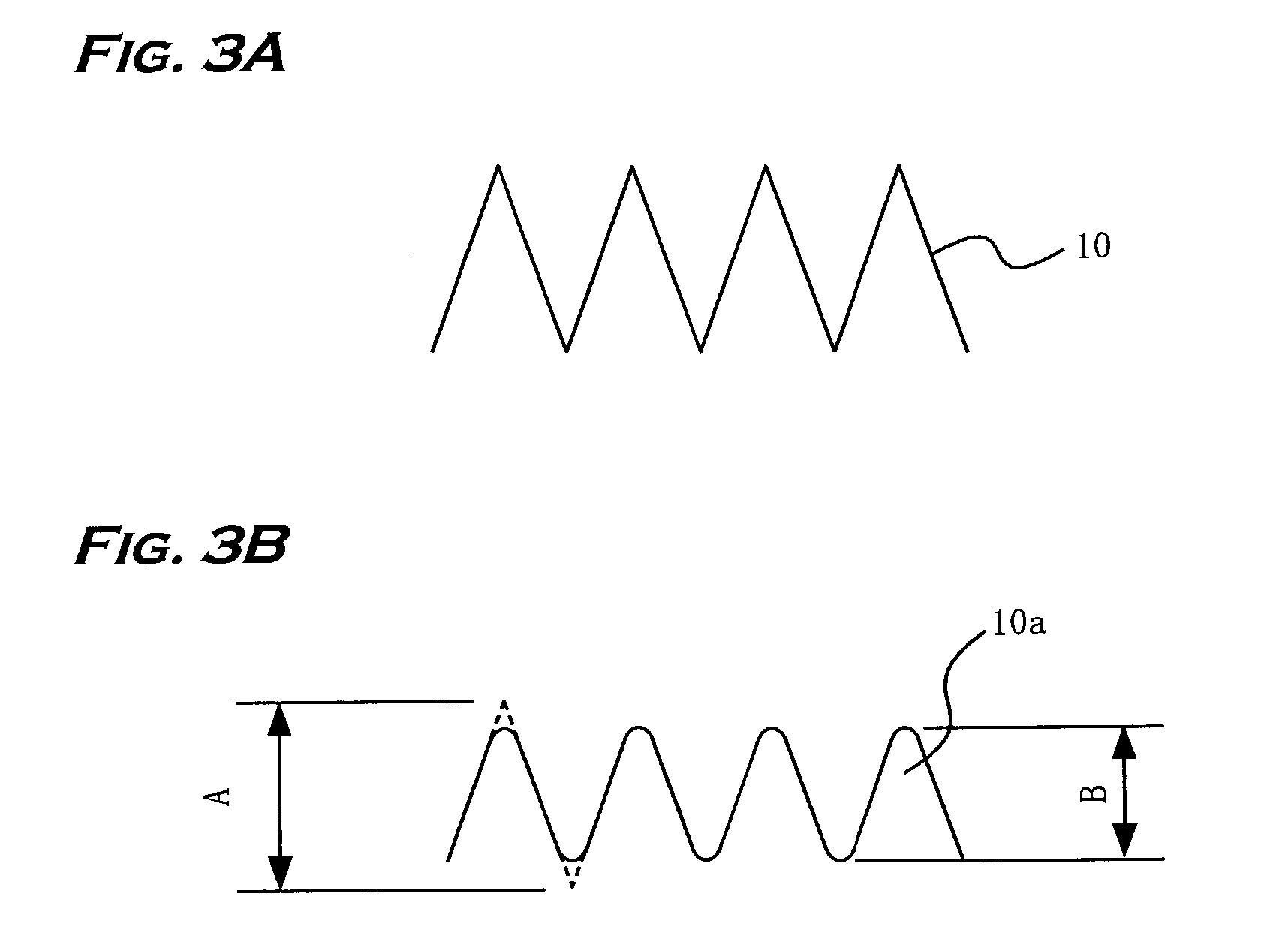
[0048]An aspect ratio is defined as a ratio D / p; a height D of the pattern to a pitch p of the pattern, shown in FIG. 2.

[0049]FIG. 4 shows a simulation result of spectral characteristics when changing the aspect ratio of the pyramid pattern. Eight kinds of pyramid pattern having the aspect ratio respectively of 0.6, 0.8, 0.9, 1, 1...


PUM

PropertyMeasurementUnit
transparentaaaaaaaaaa
aspect ratioaaaaaaaaaa
reflectanceaaaaaaaaaa

Abstract

An antireflective member with stability and a low reflectance at low cost may be provided by performing an antireflective treatment to a substrate in a molding process of the substrate. A roughened surface with a continuous pattern in a fine pyramidal shape is formed on a surface of a transparent substrate, the roughened surface is a diffraction surface with zeroth-order diffraction to visible light, and the pattern of the roughened surface is transferred from a mold at a transfer rate of not less than 70%.

Description

BACKGROUND OF THE INVENTION[0001]1. Field of the Invention[0002]This invention relates to an antireflective member used in various optical devices such as a spectroscopic analysis, optical electronics, optical communications and lighting equipment and suitably used to prevent light having wavelengths in the visible range from reflecting.[0003]2. Description of Prior Art[0004]Conventional optical elements using transparent substrates such as glasses and plastics are subjected to a surface treatment, for example an antireflective film provided on a light incident surface of the substrate, in order to reduce the amount of light reflected from the surface. A multilayered film with thin dielectric films deposited is well known as the antireflective film for light of wavelengths in the visible range. Such a multilayered film is formed by growing thin films of metal oxides etc. on a surface of a transparent substrate by means of a vacuum evaporation method or the like.[0005]Another techniq...

Claims


Application Information

Patent Timeline
Patent Type & Authority Patents(United States)
IPC IPC(8): B29D11/00B29C33/42G02B5/02G02B1/11G02B1/118G02F1/1335
CPCG02B1/11G02B1/118Y10T428/1036Y10T428/10Y10T428/24355G02F1/133502G02B1/18C09K2323/03C09K2323/00
Inventor YAMASHITA, HIROSHIMAENO, YOSHIAKI
Owner SANYO ELECTRIC CO LTD
Why Eureka
Try Eureka