Laser thermal annealing of lightly doped silicon substrates

a technology of silicon substrates and thermal annealing, applied in the direction of optical radiation measurement, instruments, manufacturing tools, etc., can solve the problem that the approach works well only on relatively heavily doped substrates

Active Publication Date: 2006-08-29
VEECO INSTR
View PDF9 Cites 74 Cited by
  • Summary
  • Abstract
  • Description
  • Claims
  • Application Information

AI Technical Summary

Problems solved by technology

However, this approach works well only on relatively heavily doped substrates (i.e., a dopant concentration of about 3×10¹⁷ atoms / cm3 or greater), where the absorption length of the laser radiation in the doped silicon is less than or roughly comparable to the thermal diffusion length.

Method used


Image

  • Laser thermal annealing of lightly doped silicon substrates
  • Laser thermal annealing of lightly doped silicon substrates
  • Laser thermal annealing of lightly doped silicon substrates

Examples


Embodiment Construction

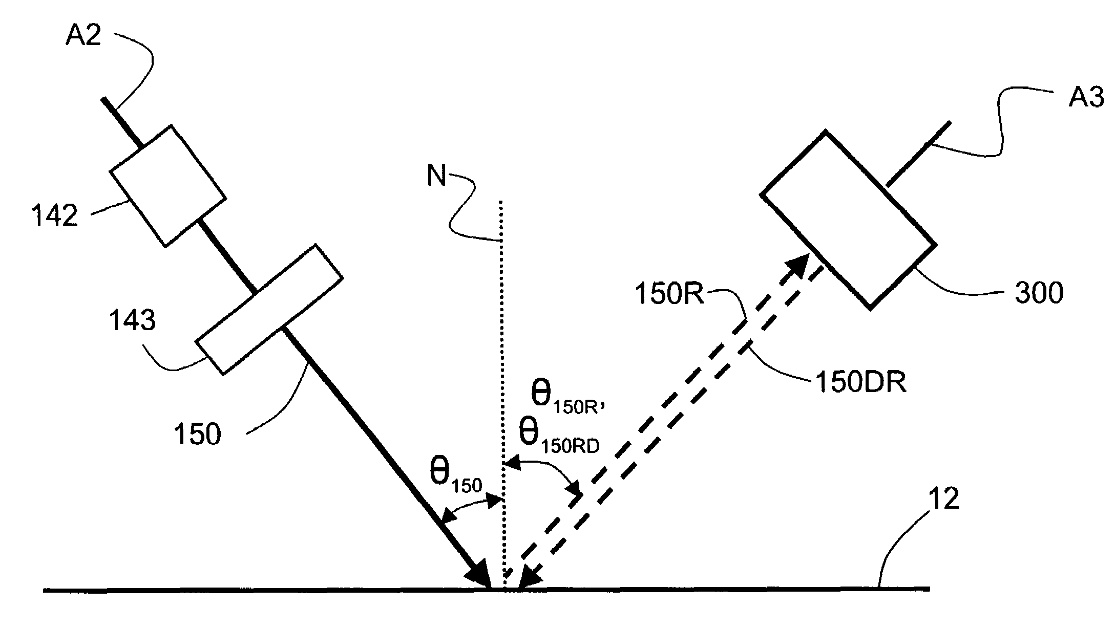
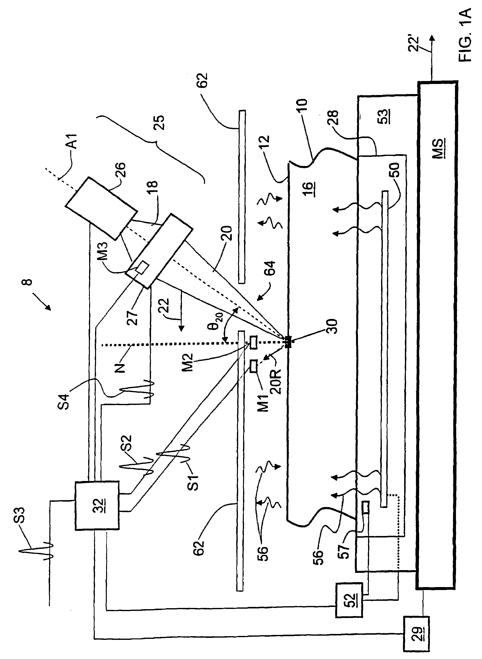
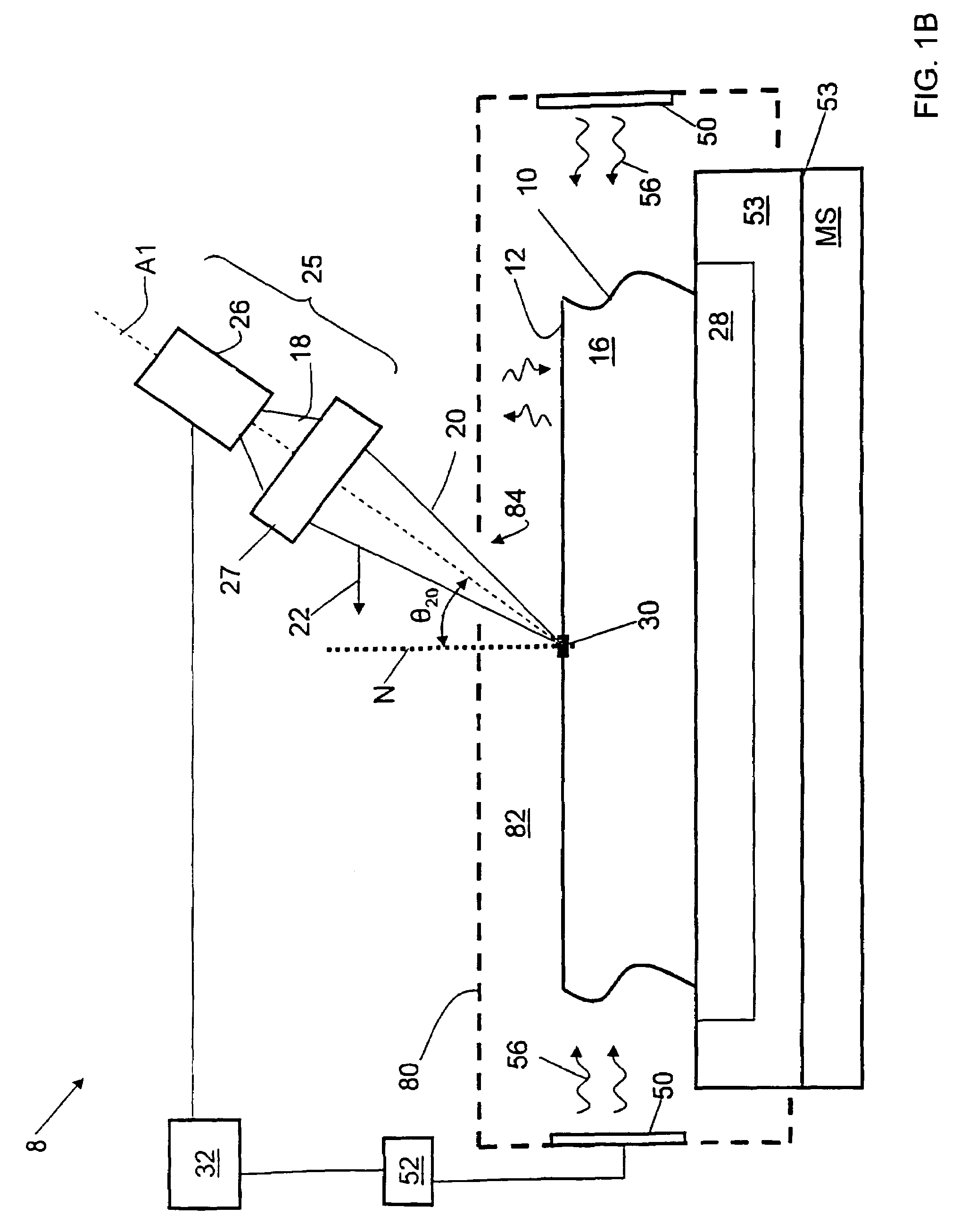
[0035]The present invention relates to laser thermal annealing (LTA) of substrates and in particular relates to apparatus and methods for performing LTA of lightly doped silicon wafers (substrates). The term “lightly doped” means herein a dopant concentration of about 1016 atoms / cm3 or less. The dopant concentration in the substrate may be that associated with normal substrate production to achieve a desired resistivity level and substrate type (i.e., N-type or P-type).

[0036]In the description below, a generalized embodiment of the LTA apparatus of the present invention is described, along with a description of the “self-sustaining annealing condition” sought to be created by the present invention. This is followed by various example embodiments of the invention. The invention is further explained in connection with a number of different substrate temperature plots that illustrate key properties of the absorption of radiation by silicon substrates. Methods of determining the appropr...


PUM

PropertyMeasurementUnit
wavelengthaaaaaaaaaa
diffusion length LDaaaaaaaaaa
absorption lengthaaaaaaaaaa

Abstract

Apparatus and method for performing laser thermal annealing (LTA) of a substrate using an annealing radiation beam that is not substantially absorbed in the substrate at room temperature. The method takes advantage of the fact that the absorption of long wavelength radiation (1 micron or greater) in some substrates, such as undoped silicon substrates, is a strong function of temperature. The method includes heating the substrate to a critical temperature where the absorption of long-wavelength annealing radiation is substantial, and then irradiating the substrate with the annealing radiation to generate a temperature capable of annealing the substrate.

Description

CROSS-REFERENCE TO RELATED APPLICATIONS[0001]This application is a Continuation-In-Part of U.S. patent application Ser. No. 10 / 674,106, filed on Sep. 29, 2003.BACKGROUND OF THE INVENTION[0002]1. Field of the Invention[0003]The present invention relates to laser thermal annealing, and in particular relates to apparatus and methods for performing laser thermal annealing of substrates that do not efficiently absorb the annealing radiation beam at ambient temperatures.[0004]2. Description of the Prior Art[0005]Laser thermal annealing or LTA (also referred to as “laser thermal processing”) is a technique used to quickly raise and lower the temperature of the surface of a substrate to produce a change in properties. An example might include annealing and / or activating dopants in the source, drain or gate regions of transistors used to form integrated devices or circuits. LTA can also be used to form silicide regions in integrated devices or circuits, to lower poly-silicon runner resistanc...

Claims


Application Information

Patent Timeline
Patent Type & Authority Patents(United States)
IPC IPC(8): H01L21/324B23K26/06B23K26/42H01L21/20H01L21/268
CPCB23K26/0604B23K26/0608H01L21/268H01L21/2026B23K26/421B23K2201/40B23K26/60B23K2101/40
Inventor TALWAR, SOMITMARKLE, DAVID A.
Owner VEECO INSTR
Why Eureka
Try Eureka