Image pickup device with high contrast detection capability

a pickup device and detection capability technology, applied in the field of image pickup devices, can solve the problems of difficult to obtain sufficient contrast in both brighter and darker portions of the field of view at the same time, and the sensibility of human vision is much inferior, so as to achieve excellent imaging, close human perceptual ability, and sufficient contrast

Inactive Publication Date: 2006-08-29
EXPL OF NEXT GENERATION
View PDF8 Cites 2 Cited by
  • Summary
  • Abstract
  • Description
  • Claims
  • Application Information

AI Technical Summary

Benefits of technology

[0035]A main advantage of the present invention is, therefore, that an image with a large luminance difference in the same field of view, which was difficult to be detected by the conventional image sensor, can be detected with sufficient contrast. As a result, the image pickup device (image sensor) of the present invention can be used as an excellent imaging device that is close to human perceptual capability. Hence, the image sensor is advantageous in the field of monitoring devices, cameras mounted on cars and the like that requires adaptation to severe environmental changes.
[0036]Considering that a CMOS image sensor in general has an S / N ratio of approximately 60 to 65 dB, the image pickup device (image sensor) of the present invention would likely be able to detect sufficient contrast for an entire screen up to the average luminance difference of approximately several hundred times, if the image quality of approximately 20 dB is allowed in the darkest portion on the screen.
[0037]Furthermore, the image pickup device (image sensor) of the present invention allows compact mounting of a function of modulating a receiving-light sensitivity characteristic by analog modulation per pixel. Thus, sensitivity and resolution no less than those of the conventional image sensor can be obtained.

Problems solved by technology

The sensing capability of an image pickup device, however, is much inferior to the sensibility of human vision.
By contrast, in a conventional image pickup device, all pixels had the same receiving-light sensitivity characteristic, which made it difficult to obtain sufficient contrast in both brighter and darker portions in the field of view at the same time.
In the conventional image pickup device, however, when a receiving-light sensitivity characteristic is adjusted to allow the inside to be seen, the outside of the window becomes too bright, so that contrast in a brighter portion cannot be detected, as shown in the example shot in FIG. 14.
This reveals that the conventional image sensor is much inferior to human vision in detection of sufficient contrast in the entire region when there are brighter and darker portions present at the same time in the field of view.
The low contrast sensibility is one of major problems to be solved in order to practically use the conventional image pickup device as a device for detecting visual information that substitutes for human vision.
Moreover, in a dark portion, contrast will also be insufficient, since the amplitude is lowered to one-fifth of the whole.
Thus, the conventional image pickup device cannot detect sufficient contrast even in a scene we often come across in everyday life.

Method used


Image

  • Image pickup device with high contrast detection capability
  • Image pickup device with high contrast detection capability
  • Image pickup device with high contrast detection capability

Examples


first embodiment

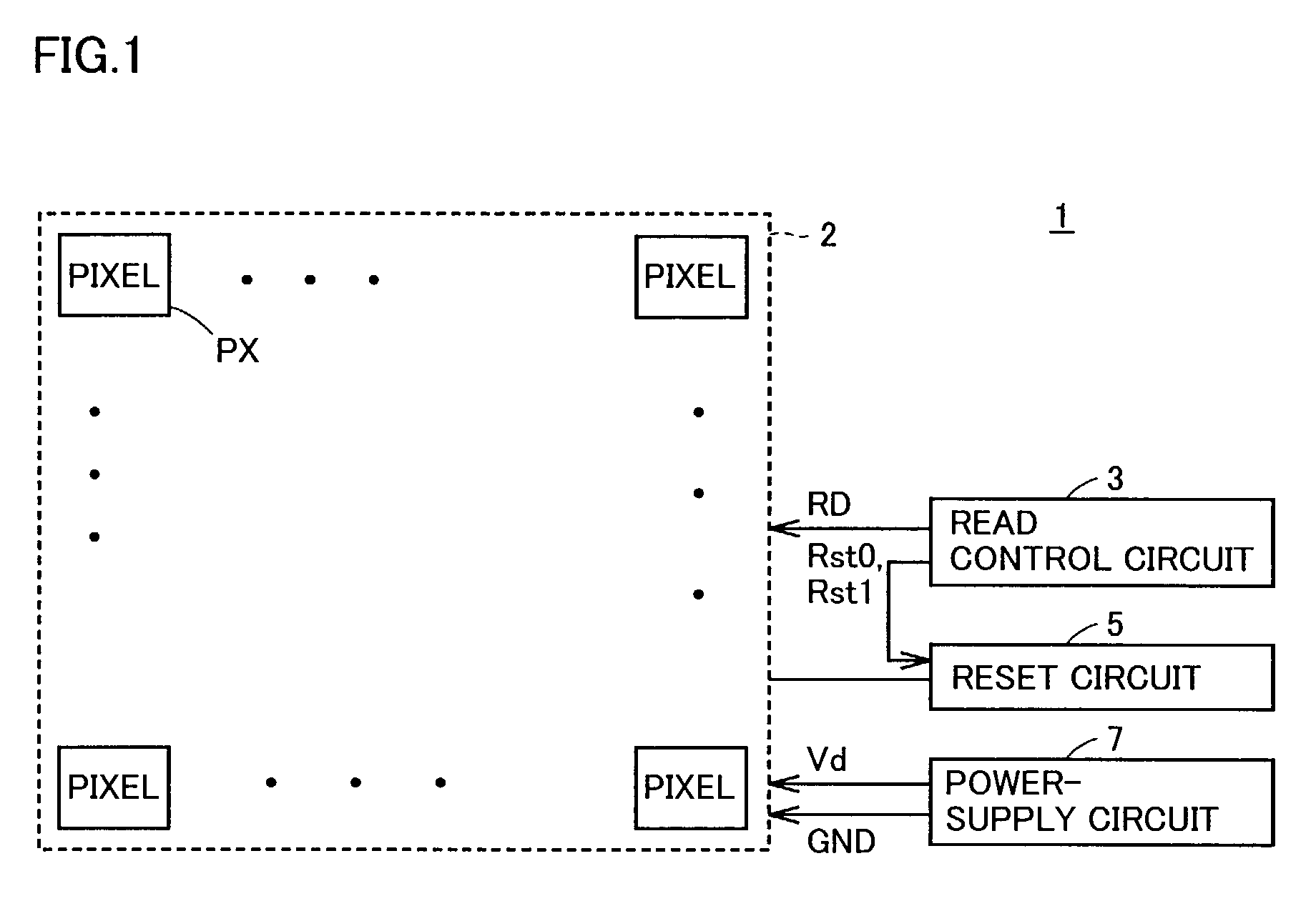
[0056]Referring to FIG. 1, an image pickup device 1 according to the present invention includes a pixel array 2 in which a plurality of pixels PX are arranged in a matrix of rows and columns, a read control circuit 3, a reset circuit 5 and a power-supply circuit 7.

[0057]Read control circuit 3 generates a control signal RD for controlling timing of image data generation in pixel array 2. Reset circuit 5 periodically resets the state of a receiving-light detecting element in each pixel PX. The timing of resetting operation by reset circuit 5 is controlled by reset signals Rst0, Rst1 from read control circuit 3. Power-supply circuit 7 supplies a power-supply voltage Vd and a ground voltage GND to each pixel in pixel array 2.

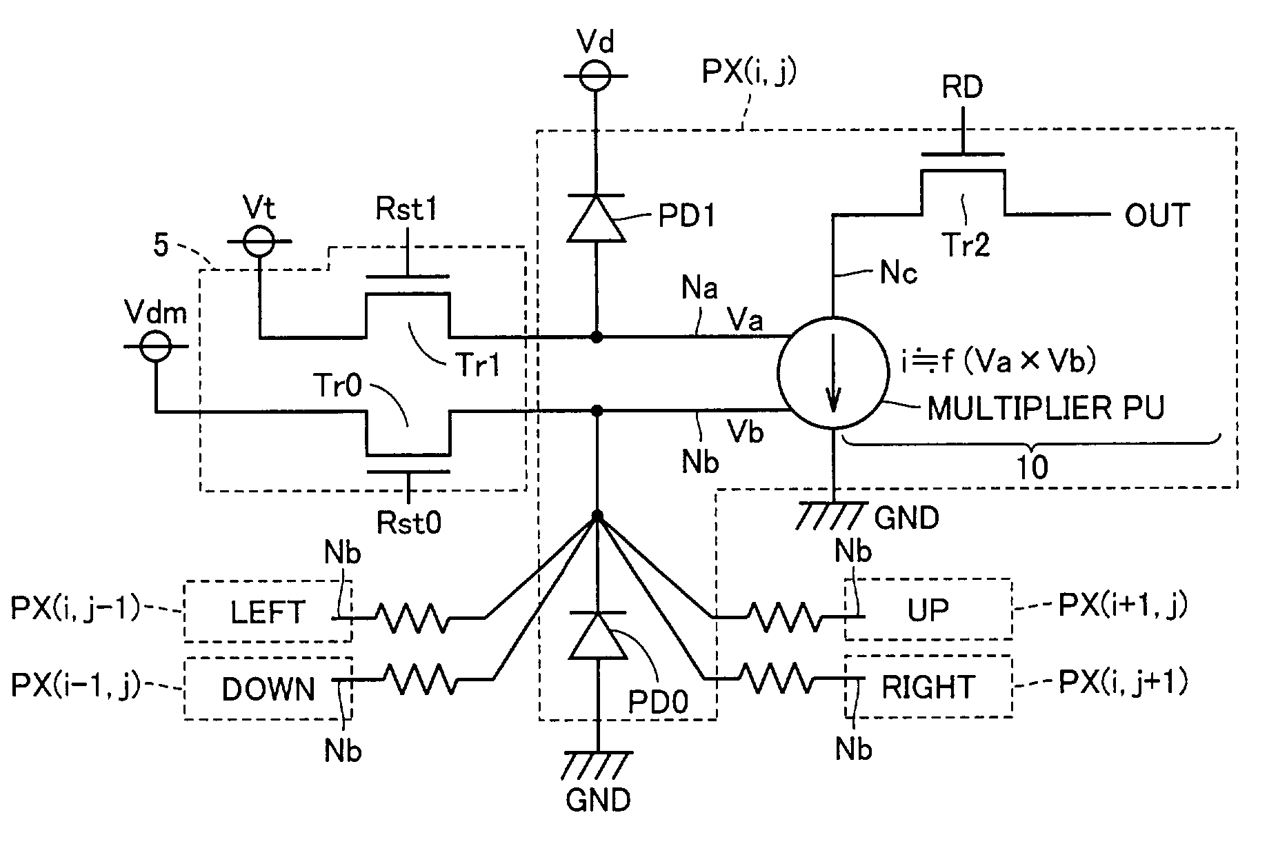
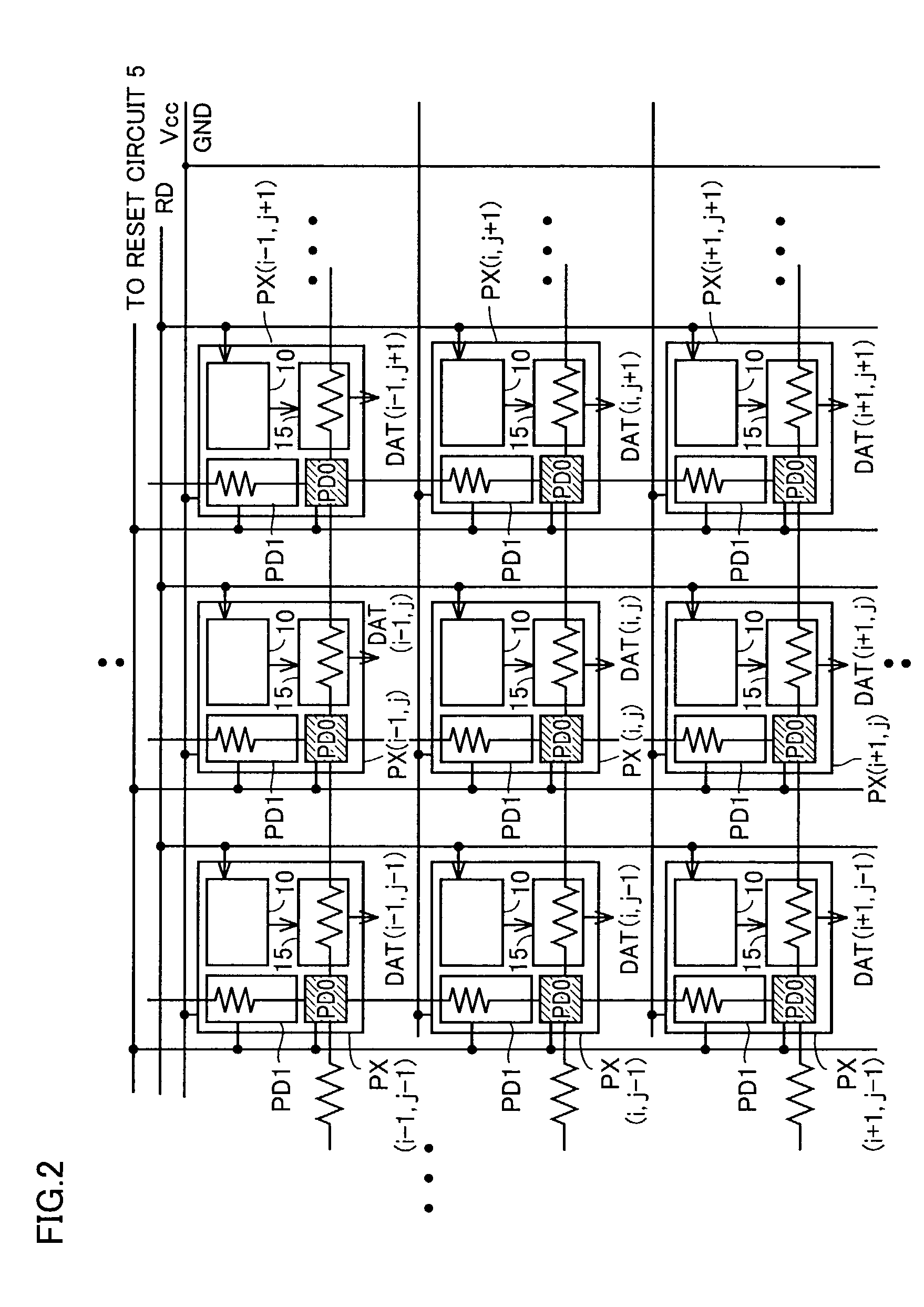
[0058]FIG. 2 is a block diagram illustrating a configuration of each pixel. In FIG. 2, pixel PX (i, j) in the i-th row and the j-th column (i, j: natural numbers) and pixels adjacent thereto are representatively shown among the plurality of pixels arranged in rows a...

second embodiment

[0078]In the second embodiment, a configuration of multiplier PU suitable for such control of the signal amplification factor will be described. In the second embodiment, an MOS transistor that can control a gain coefficient β in accordance with an input voltage to a control gate (hereinafter also referred to as “A-MOS (Adjustable β-MOS) device”) is used to realize the function of automatically adjusting a receiving-light sensitivity characteristic per pixel.

[0079]Referring to FIG. 5, the A-MOS device includes, in addition to a normal gate GR, a source SR and a drain DR that are similar to those in a normal MOS transistor, a control gate CG formed at a certain angle with the normal gate.

[0080]FIG. 6 is a schematic view showing parameters for configuration of the A-MOS device.

[0081]Referring to FIG. 6, the A-MOS device has, as configuration parameters, a gate length Lr and a gate width Wr of normal gate GR, and an angle θ formed by normal gate GR and control gate CG.

[0082]FIGS. 7A an...

third embodiment

[0092]In the third embodiment, effective arrangement of two photodiodes provided in each pixel will be described.

[0093]FIG. 9 is a structural view showing an arrangement example of photodiodes according to the third embodiment.

[0094]Referring to FIG. 9, a PN junction formed between a P-type silicon substrate (P-sub) 20 on which an image pickup device is formed and an N-well 21 provided on P-type silicon substrate 20 is used to form photodiode PD0 for detecting an average amount of light in a peripheral region.

[0095]Further, a PN junction formed between a P+ region 22 formed within N-well 21 and N+ region 23 formed within P+ region 22 is used to form photodiode PD1 for detecting an amount of light entering into the corresponding pixel. It is noted that P+ region 22 and N+ region 23 are heavily doped compared to P-type silicon substrate 20 and N-well 21.

[0096]P+ region 22 and N+ region 23 are provided independently for each pixel. Further, a plurality of pixels created in the same N-w...


PUM


Abstract

Each pixel includes first and second photodiodes that are receiving-light detecting elements. The first photodiode applies a first potential according to an amount of light entering into the corresponding pixel. An internal node is electrically coupled with an internal node in another pixel via a resistance component. Hence, the second photodiode applies a second potential according to an average amount of light on the periphery to the corresponding internal node. A pixel signal generating circuit reads out a multiplied result of the first and second potentials as a pixel signal. The pixel signal has an intensity corresponding to the amount of light in the pixel in accordance with a receiving-light sensitivity characteristic (signal amplification factor) that is automatically adjusted based on an average amount of light in a region on the periphery of the pixel.

Description

BACKGROUND OF THE INVENTION[0001]1. Field of the Invention[0002]The present invention relates to an image pickup device that realizes receiving-light sensitivity characteristic that is close to the sensibility of human vision, and more particularly, to an image pickup device that can detect sufficient contrast in an entire region even if there is an area with a large difference in luminance present in a field of view. Hence, the inventive technique can be utilized in various situations for an imaging device having high visual sensibility, such as a monitoring camera for an area including outdoors, a camera that is mounted on a car and the like.[0003]2. Description of the Background Art[0004]Solid-state imaging devices such as CCD (Charge-Coupled Device) and CMOS (Complementary Metal-Oxide Semiconductor) imagers, i.e. semiconductor image sensors (hereinafter also referred to as “image pickup device”), have been embedded in video cameras, digital cameras, and nowadays even in a mobile...

Claims


Application Information

Patent Timeline
Patent Type & Authority Patents(United States)
IPC IPC(8): H04N3/14H04N5/335H01L27/146H04N5/355H04N5/369H04N5/374H04N5/3745
CPCH01L27/14603H04N25/59H04N25/77H04N3/155
Inventor ARIMA, YUTAKA
Owner EXPL OF NEXT GENERATION
Why Eureka
Try Eureka