

Fractal structure and its forming method
a fractal structure and forming method technology, applied in the direction of magnetism bodies, crystal growth processes, polycrystalline material growth, etc., can solve the problems of high integration difficulties, physical properties of materials, and restricted applications of such electronic circuits, and achieve the effect of improving controllability
- Summary
- Abstract
- Description
- Claims
- Application Information
AI Technical Summary
Benefits of technology
Problems solved by technology
Method used
Image

Examples
first embodiment
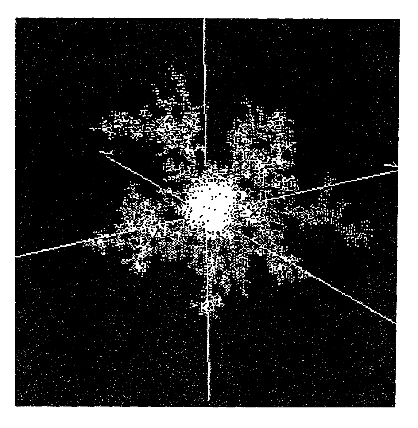
(1) Formation of a Stellar Fractal Structure
[0072]A method of forming a stellar fractal structure according to the first embodiment can be obtained by developing Dielectric Breakdown Model ((32) A. Erzan, L. Pietronero, A. Vespignani, Rev. Mod. Phys. 67, 545 (1995); (33) L. Niemeyer, L. Pietronero, H. J. Wiesmann, Phys. Rev. Lett. 52, 1033 (1984)).
[0073]Here is defined a cubic lattice S in a three-dimensional space, and a scalar potential field φ(i1, i2, i3) is defined on its lattice site (i1, i2, i3)∈S and called a potential. Let this potential obey the Laplace's equation
Δφ(i1,i2,i3)=0 (1)
A pattern Tn, which will be defined later, is a set of lattice sites on the three-dimensional lattice. To contains (0, 0, 0) alone, and Tn+1 is created by sequentially adding a single lattice site to Tn according to the rule given below.
[0074]Let the potential of each site contained in Tn be I and let the potential at infinity be 0. That is,
φ(i1,i2,i3)=0 when (i1,i2,i3)→∞ (2)
φ(i1,i2,i3)=1 when (...
second embodiment
(1) Formation of a Stellar Fractal Structure
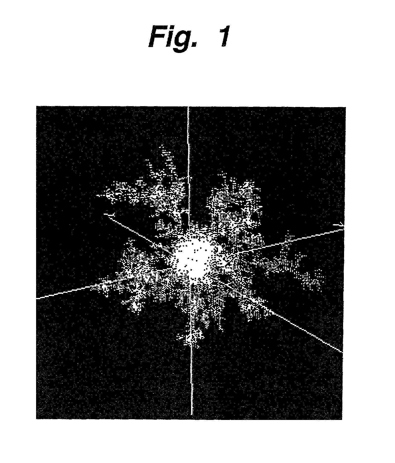
[0100]A method of forming the star-shaped fractal structure according to the second embodiment is the same as the method of forming the stellar fractal structure according to the first embodiment. As growth conditions, however, (α1, α2)=(0, 1) and (α1, α2)=(1, 2) were used in addition to (α1, α2)=(0, 2), and numerical experiment of growth was conducted for these cases.
[0101]In FIGS. 9 through 11, for respective examples obtained by the growth experiment, log—log plotting was made similarly to the first embodiment. (α1, α2)=(0, 2) was used in FIG. 9, (α1, α2)=(0, 1) was used in FIG. 10, and (α1, α2)=(1, 2) was used in FIG. 11. As shown in FIGS. 9 through 11, when log(r) is small, plots ride on a straight line with a large inclination. When log(r) exceeds a certain critical point, plots ride on a straight line with a small inclination. This means that the structure includes two different fractal dimensions. The site of the critical point inc...
third embodiment
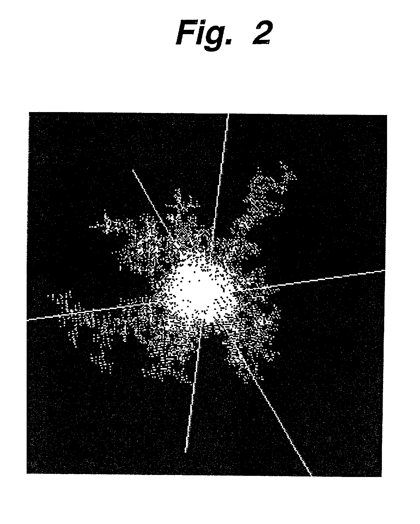
(1) Formation of a Stellar Fractal Structure
[0113]A method of forming the star-shaped fractal structure according to the third embodiment is the same as the method of forming the stellar fractal structure according to the first embodiment. As growth conditions, however, similarly to the second embodiment, (α1, α2)=(0, 1) and (α1, α2)=(1, 2) were used in addition to (α1, α2)=(0, 2), and numerical experiment of growth was conducted for these cases. Results of log—log plotting for respective cases obtained by the growth experiment are the same as those shown in FIGS. 9 through 11.
(2) Electron System on a Stellar Fractal Structure
[0114]Let us define a quantum system of one particle on the stellar fractal defined in (1). Assume a lattice site shown below, which is the origin of Tn.
rp=(i1,p,i2,p,i3,p)εTn (44)
where p=0, 1, 2, . . . , n. Here is defined an operator ĉp† that creates a quantum at a lattice site rpεTn. Of course, an anticommutative relation
{ĉp,ĉq}=δp,q (45)
is established. He...
PUM
 Abstract
Description
Claims
Application Information