Supercharge Your Innovation With Domain-Expert AI Agents!

Method for forming conductive line of semiconductor device

a technology of conductive lines and semiconductors, applied in the direction of semiconductor devices, basic electric elements, electrical equipment, etc., can solve problems such as degradation of device characteristics, and achieve the effect of improving device reliability and stabilizing contact characteristics

Active Publication Date: 2006-09-05
MOSAID TECH
View PDF8 Cites 3 Cited by
  • Summary
  • Abstract
  • Description
  • Claims
  • Application Information

AI Technical Summary

Benefits of technology

This approach effectively stabilizes contact resistance across all regions, enhancing the reliability and performance of semiconductor devices by reducing variations and maintaining moderate contact resistance values, thereby improving device characteristics.

Problems solved by technology

In case of a highly integrated and high-speed semiconductor device, a tungsten bit line having low resistance is used instead since this structure has a limitation due to high sheet resistance.
However, increase in the thickness of the Ti film increase the contact resistance of P+ region as described above, resulting in a degradation of device characteristic.

Method used


Image

  • Method for forming conductive line of semiconductor device
  • Method for forming conductive line of semiconductor device
  • Method for forming conductive line of semiconductor device

Examples


Embodiment Construction

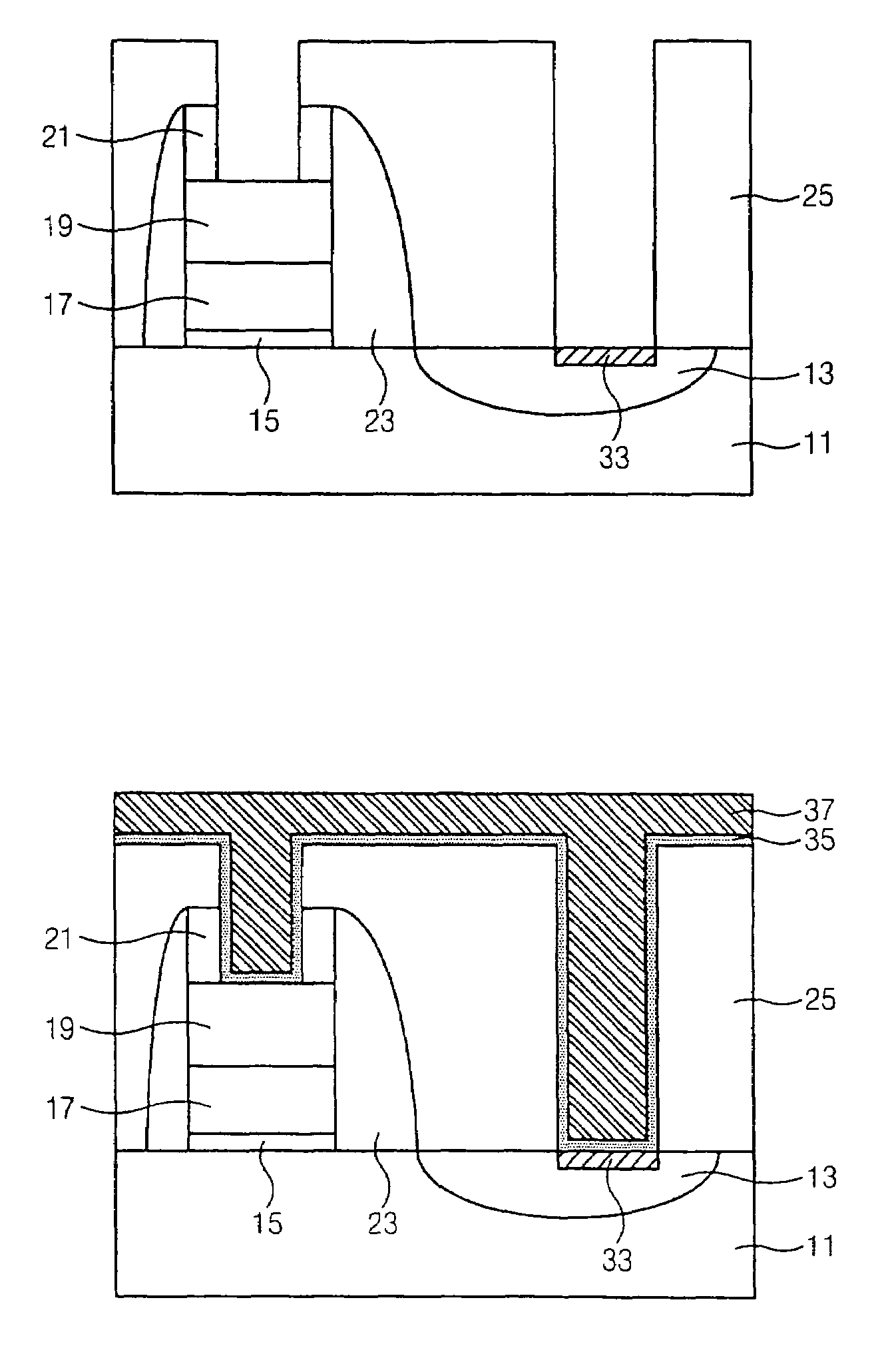
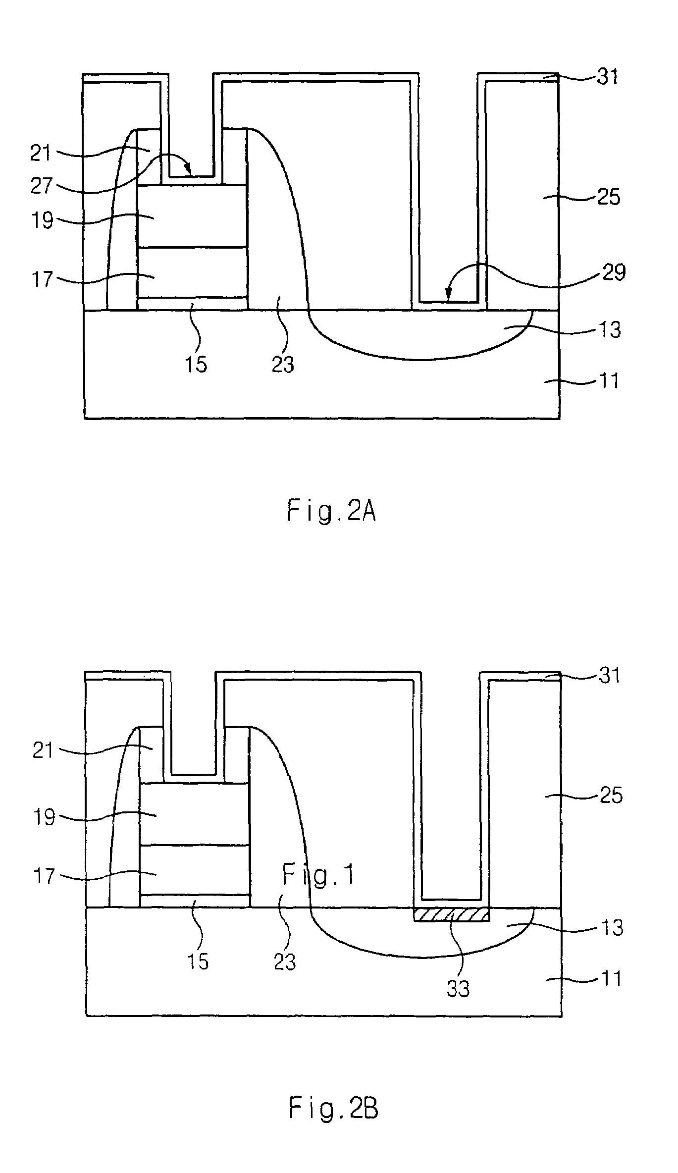
[0015]A method for forming conductive line of semiconductor device in accordance with a preferred embodiment of the present invention will now be described in detail with reference to the accompanying drawings.

[0016]FIGS. 2A through 2D are cross-sectional diagrams illustrating method for forming conductive line of semiconductor device in accordance with the present invention.

[0017]Referring to FIG. 2A, a device isolation film (not shown) for defining an active region is formed on a semiconductor substrate 11.

[0018]Thereafter, a stacked structure of a gate oxide film 15, a polysilicon film 17 for gate electrode, a tungsten silicide layer 19 and a hard mask film 21 is formed on the semiconductor substrate 11. The stacked structure is then etched to form a gate electrode.

[0019]Next, an n-type or a p-type impurity is ion-implanted in the semiconductor substrate 11 using the gate electrode as an implant mask to form an impurity junction region 13.

[0020]Thereafter, an insulating film (not...


PUM


Abstract

A method for conductive line of semiconductor device is disclosed. A cobalt silicide layer is formed on an impurity junction region exposed through a contact hole. The cobalt silicide layer stabilizes a contact resistance so that the contact resistance of the impurity junction region does not vary in subsequent thermal processes.

Description

BACKGROUND OF THE INVENTION[0001]1. Field of the Invention[0002]The present invention relates to method for forming conductive line of semiconductor device, and in particular to an improved method for forming conductive line of semiconductor device which provides improved contact resistance characteristics.[0003]2. Description of the Background Art[0004]A bit line structure, which is a data I / O path of semiconductor device, comprises a polycide structure consisting of a polysilicon layer and a tungsten silicide layer. In case of a highly integrated and high-speed semiconductor device, a tungsten bit line having low resistance is used instead since this structure has a limitation due to high sheet resistance.[0005]Resistance stabilization is required for the tungsten bit lone because the contact resistance varies by the subsequent thermal processes.[0006]Generally, the contact resistance is greatly increased during a subsequent thermal process in a P+ region where a thick Ti film is ...

Claims


Application Information

Patent Timeline
Patent Type & Authority Patents(United States)
IPC IPC(8): H01L21/44H01L21/28H01L21/285H01L21/3205H01L21/336H01L21/4763H01L21/74H01L21/768H01L21/8238
CPCH01L21/743H01L21/28518H01L21/28
Inventor JIN, SUNG GON
Owner MOSAID TECH
Features
  • R&D
  • Intellectual Property
  • Life Sciences
  • Materials
  • Tech Scout
  • Unparalleled Data Quality
  • Higher Quality Content
  • 60% Fewer Hallucinations
Learn More