

Envelope follower end point detection in time division multiplexed processes
a follower end point and time division multiplexing technology, applied in semiconductor/solid-state device testing/measurement, fluid pressure measurement, instruments, etc., can solve the problem of reducing the thickness of the underlying stop layer, and affecting the detection accuracy of envelope follower end points
- Summary
- Abstract
- Description
- Claims
- Application Information
AI Technical Summary
Benefits of technology
Problems solved by technology
Method used
Image

Examples
Embodiment Construction
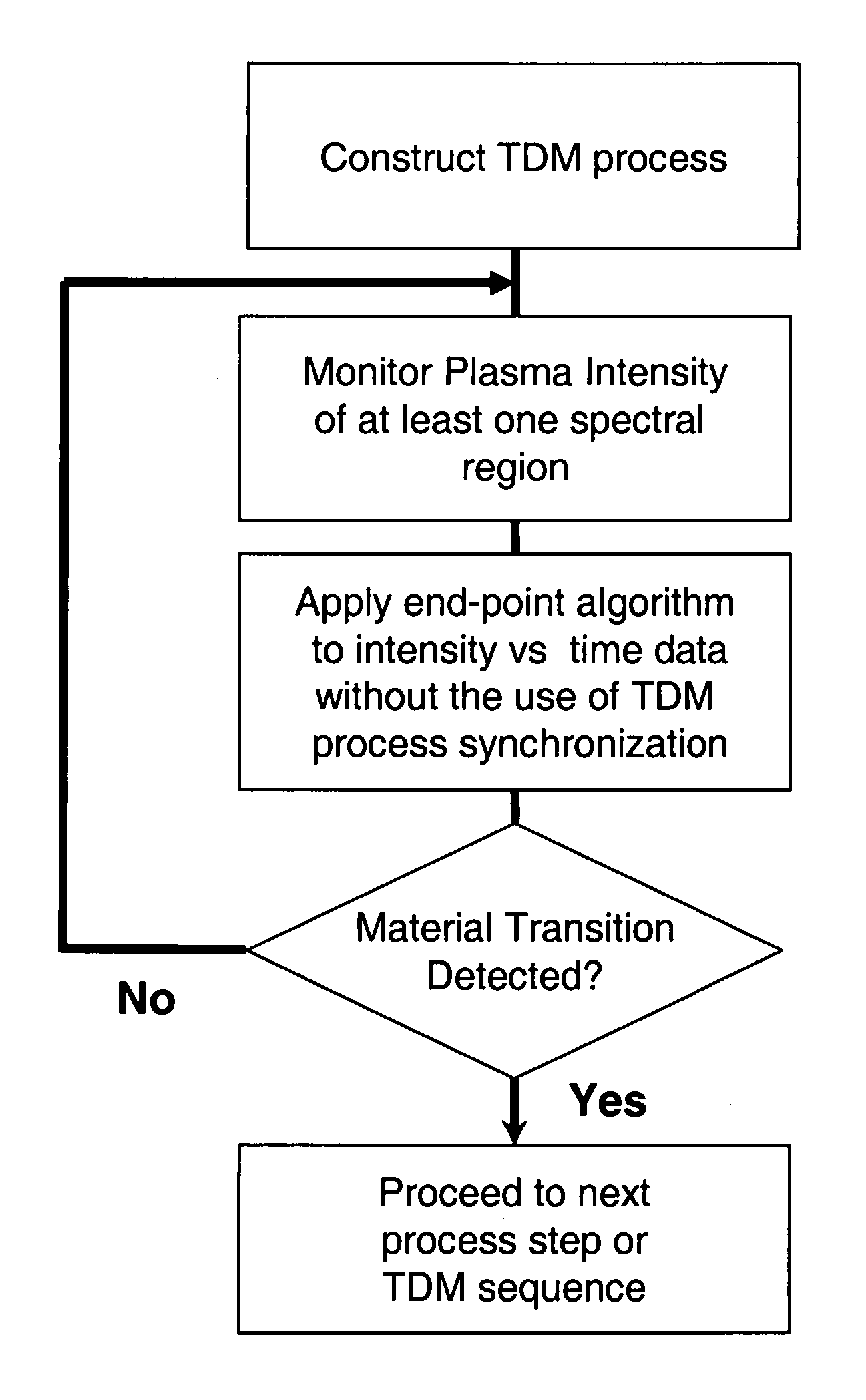
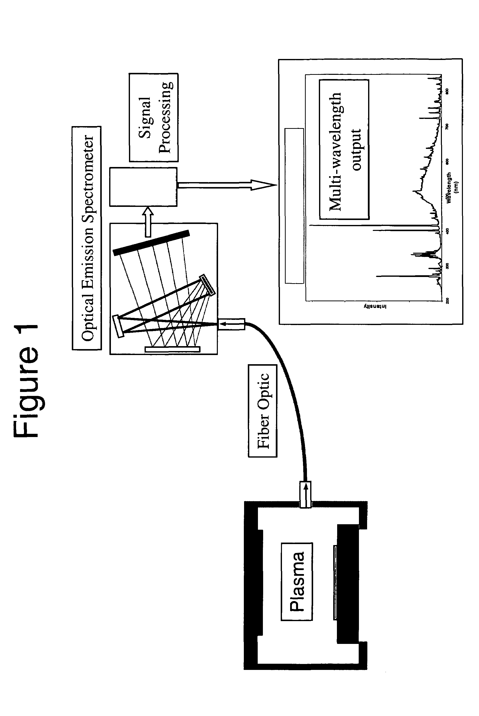
[0052]We disclose a means of detecting the transition between different materials in a time division multiplexed (TDM) process by analyzing the intensity of at least one wavelength region of the plasma emission without the use of a synchronizing trigger.
[0053]Due to the periodic and repeating nature of a TDM process, by design, the process has a number of characteristic frequencies associated with it. As an example, consider a two step TDM silicon etch process consisting of a five second etch step and a five second deposition step that are subsequently repeated a number of times (see Table 1 below). One characteristic frequency will be 0.1 Hz, determined by the total cycle time (10 seconds).
[0054]
TABLE 1ProcessUnit ofParameterMeasureDepositionEtchSF6 Flowsccm0.5100C4F8 Flowsccm700.5Ar Flowsccm4040PressuremTorr2223RF Bias PowerW112ICP PowerW10001000Step Timeseconds55
Note the deposition and etch steps differ in chemistry, RF bias power and pressure resulting in significantly different...
PUM
| Property | Measurement | Unit |
|---|---|---|
| wavelength | aaaaa | aaaaa |
| frequency | aaaaa | aaaaa |
| frequency | aaaaa | aaaaa |
Abstract
Description
Claims
Application Information