Device for preventing intensity reduction of optical signal, optical emission spectrometer, optical instrument, and mass spectrometer including the same

a technology of optical signal and intensity reduction, applied in the direction of optical radiation measurement, instruments, particle separator tube details, etc., can solve the problems of reducing the sensitivity of receiving a measuring instrument, unable to measure plasma, and reducing the measured intensity of optical signal, so as to prevent the intensity reduction of optical signal

Active Publication Date: 2015-05-05
IND ACADEMIC CORP FOUND YONSEI UNIV
View PDF17 Cites 11 Cited by
  • Summary
  • Abstract
  • Description
  • Claims
  • Application Information

AI Technical Summary

Benefits of technology

[0011]The present invention has been made in an effort to provide a device for preventing the intensity reduction of an optical signal capable of efficiently solving problems due to charging particles and harmful electromagnetic waves such as an RF electromagnetic wave which act as contaminants deteriorating measuring sensitivity of an optical emission spectrometer, an optical instrument, a mass spectrometer, and an optical emission spectrometer, an optical instrument, and a mass spectrometer including the same.
[0012]An exemplary embodiment of the present invention provides a device for preventing the intensity reduction of an optical signal including a shielding filter which has a mesh structure capable of blocking RF electromagnetic waves radiated from a plasma field for a wafer processing, is installed in the front of an optical window of an optical emission spectrometer for measuring the plasma field from an emission spectrum image of the plasma field, and collects charging particles passing through the mesh.

Problems solved by technology

However, when the plasma is measured by the optical techniques using the optical emission spectrometer and the like, a measured intensity of the optical signal is reduced due to contamination of a receiving optical window and as a result, the receiving sensitivity of a measuring instrument is lowered, such that it is impossible to measure the plasma in many cases.
Further, even in a device of analyzing components by absorbing gases such as the mass spectrometer, the ICP (inductively coupled plasma), and the optical emission spectrometer, since reactive ions and particles are absorbed to a detector in the absorbing process of the gas, the performance of the detector is deteriorated.
Further, since RF electromagnetic waves, ultrahigh frequencies, and the like are radiated in a plasma generation process or the generated plasma, if the insides of the optical emission spectrometer and the mass spectrometer are exposed by the harmful electromagnetic waves as it is, malfunction of communication equipment may occur, such that in order to solve the problems due to the harmful electromagnetic waves, measures are required.

Method used


Image

  • Device for preventing intensity reduction of optical signal, optical emission spectrometer, optical instrument, and mass spectrometer including the same
  • Device for preventing intensity reduction of optical signal, optical emission spectrometer, optical instrument, and mass spectrometer including the same
  • Device for preventing intensity reduction of optical signal, optical emission spectrometer, optical instrument, and mass spectrometer including the same

Examples


Embodiment Construction

[0062]Hereinafter, exemplary embodiments of the present invention will be described below with reference to the accompanying drawings.

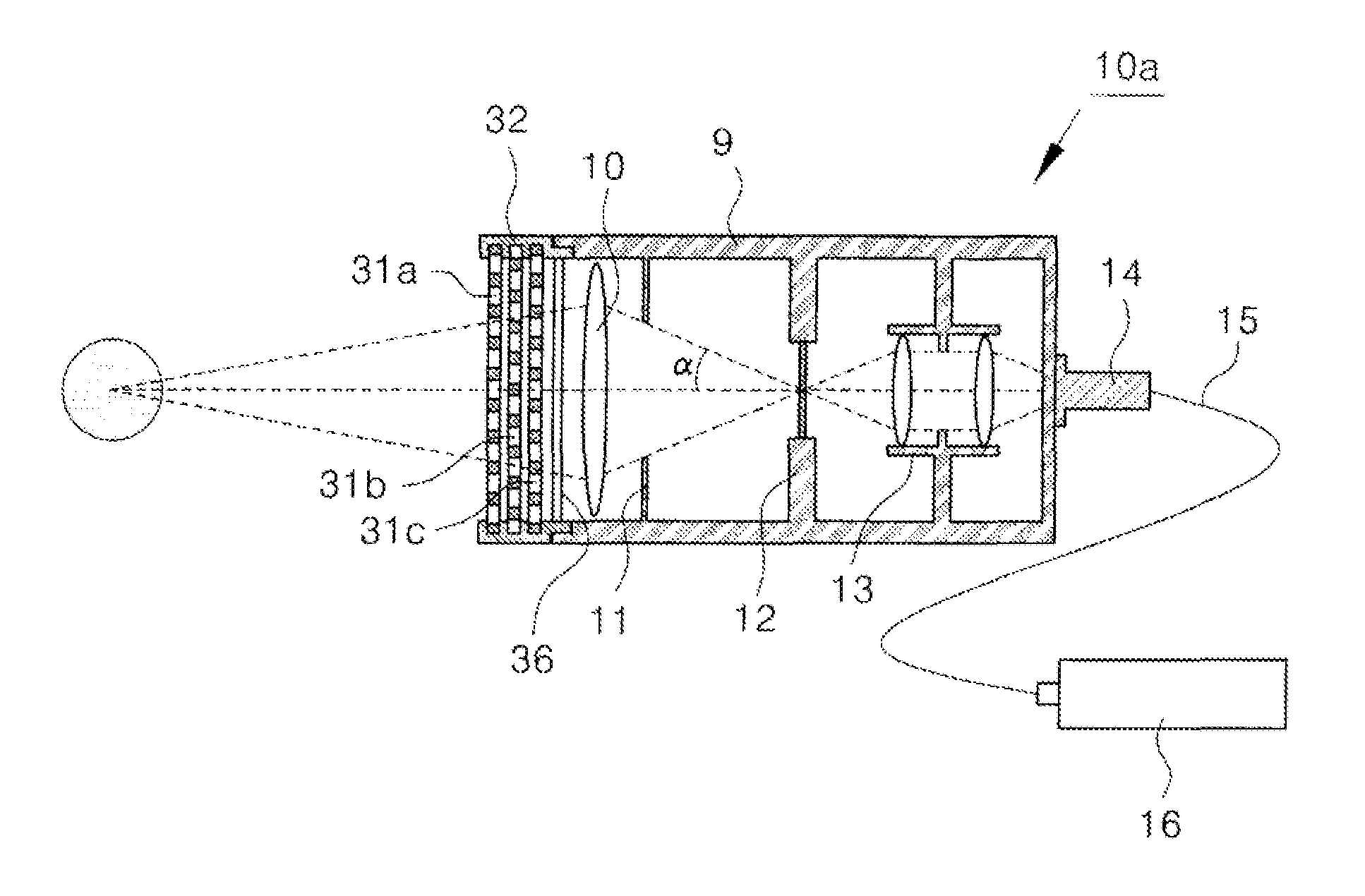
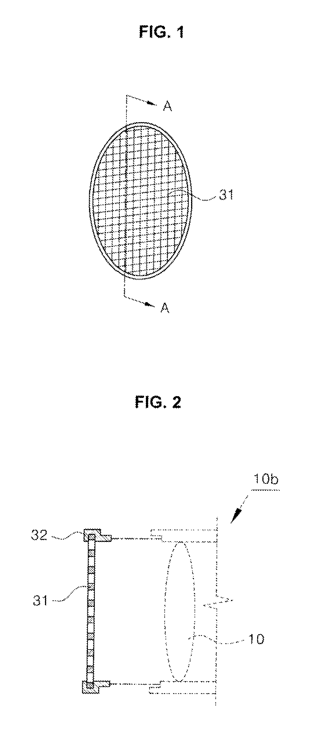
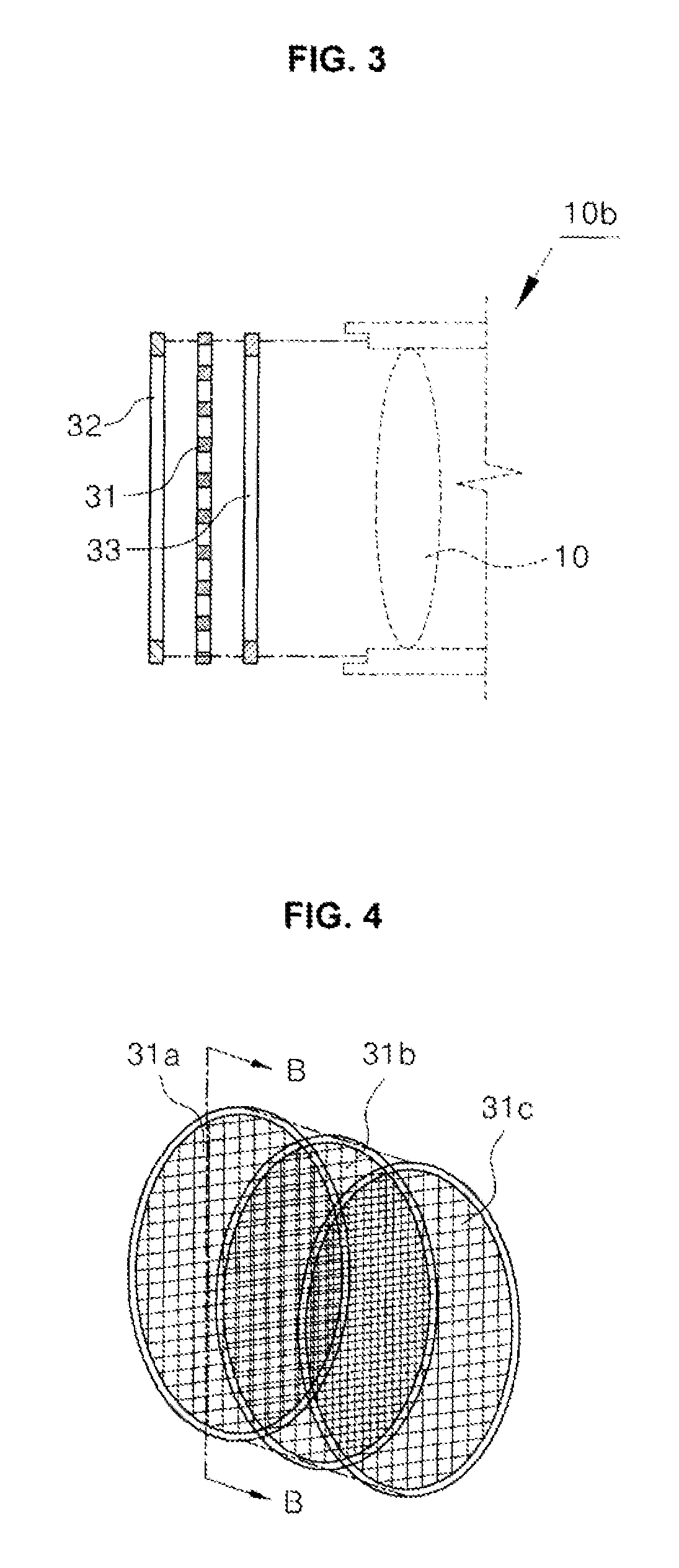
[0063]FIG. 1 is a perspective view showing a shielding filter of a device for preventing the intensity reduction of an optical signal according to a first exemplary embodiment of the present invention and FIGS. 2 and 3 are cross-sectional views showing first and second examples of a fixation frame together with a cross-section of line A-A of FIG. 1, respectively.

[0064]Referring to FIGS. 1 to 3, a device for prevention the intensity reduction of an optical signal according to an exemplary embodiment of the present invention includes a shielding filter 31 having a mesh structure capable of collecting charging particles floating on a path of an emission spectrum (hereinafter, used together with an ‘optical signal’) of a plasma field while blocking a RF electromagnetic wave radiated in the plasma field.

[0065]The shielding filter 31 is installed in the fro...


PUM


Abstract

A device for a device for preventing the intensity reduction of an optical signal, an optical emission spectrometer, an optical instrument, and a mass spectrometer including the same are provided. The device for preventing the intensity reduction includes a shielding filter which has a mesh structure capable of blocking RF electromagnetic waves radiated from a plasma field for a wafer processing, is installed in the front of an optical window of an optical emission spectrometer for measuring the plasma field from an emission spectrum image of the plasma field, and collects charging particles passing through the mesh.

Description

CROSS REFERENCE TO RELATED APPLICATION[0001]This application claims the benefit under 35 U.S.C. 119(a) of Korean Patent Application No. 10-2010-0112508, filed on Nov. 12, 2010, and Korean Patent Application No. 10-2011-0095713, filed on Sep. 22, 2011, the disclosure of each of which is incorporated by reference in its entirety for all purposes.BACKGROUND[0002]1. Technical Field[0003]The present invention relates to a device for preventing the intensity reduction of an optical signal, an optical emission spectrometer, an optical instrument, and a mass spectrometer including the same.[0004]2. Background Art[0005]In general, in a processing of wafers and the like of semiconductor elements, a plasma process is widely used and particularly, in the processing of DRAM wafers and the like which are expansively used due to universalization of PCs and the like, it is required that wafers having a size of 30 cm are produced at a high yield by the plasma process.[0006]For the processing uniform...

Claims


Application Information

Patent Timeline
Patent Type & Authority Patents(United States)
IPC IPC(8): G01J3/30G01J3/02G01J3/443H01J49/04H05K9/00
CPCG01J3/443G01J3/0286H01J49/0422H05K9/009G01J3/0229H01J49/068
Inventor HAHN, JAE WON
Owner IND ACADEMIC CORP FOUND YONSEI UNIV
Why Eureka
Try Eureka