Latch-up-free ESD protection circuit using SCR

a protection circuit and esd technology, applied in the direction of emergency protection arrangements for limiting excess voltage/current, pulse manipulation, pulse technique, etc., can solve the problems of high trigger voltage, unsatisfactory electrostatic discharge efficiency, and device damage, etc., to achieve high discharge efficiency, high stability, and fast switching

Inactive Publication Date: 2006-09-05
KING BILLION ELECTRONICS
View PDF5 Cites 13 Cited by
  • Summary
  • Abstract
  • Description
  • Claims
  • Application Information

AI Technical Summary

Benefits of technology

[0014]The main object of the present invention is to provide an ESD protection circuit that enables ESD protection for semiconductor devices but is immune to latch-up in both the fast-transient and quasi-static modes, and the ESD protection circuit also has the advantages of fast switching, high discharge efficiency, and high stability.
[0020]According to the present ESD protection circuit, when overvoltage stress develops over the input pad (PAD) in the forward fast-transient mode, the excitation over the positive power supply causes the transistor gating circuit to output a low voltage pulse and a forward voltage is generated to enable the turn-on switch. After the SCR is triggered into conduction, the voltage over the input pad (PAD) rapidly falls to a holding voltage of the SCR as the transient current flows through the circuit, and the SCR is then engaged in conduction, thus providing full protection in electrostatic discharge, and having the advantages of fast switching, high discharge efficiency, and low trigger voltage.
[0025]In the voltage clamping circuit, the Zener diode and a diode are connected back-to-back, whereby when overvoltage stress develops over the input pad (PAD) in the reverse fast-transient mode, the circuit still can provide ESD protection, and it also reduces leakage current of the Zener diode.

Problems solved by technology

When an operator touches a semiconductor device, the electrostatic charge stored on the surface of human body is transferred to the device with a burst of high voltage electrostatic charge, thus causing destructive damage to the device.
One advantage of this ESD protection circuit is that latch-up will never occur, because the forward voltage will fall rapidly below a threshold voltage of the MOSFET device as the transient current flows through the circuit, but the efficiency in electrostatic discharge has not been satisfactory.
The ESD protection circuit using the SCR provides full ESD protection for semiconductor devices, but its problem is the high trigger voltage.
However, these circuits are not all without problems.
Besides, the SCR will remain in latching after the transient current is stopped, and the circuit cannot tolerate high voltage DC.
The ESD protection circuit (DCTSCR), as shown in FIG. 10, is formed by a diode chain (D1–D4) triggered SCR, which is not only low voltage triggered, but also provides ESD protection in both fast-transient and quasi-static modes, but a more serious problem is the leakage current in forward bias.
This circuit possesses the advantages of low voltage triggering, and ESD protection in both the fast-transient and quasi-static modes, and the only problem is that it takes longer time to be turned on.
In conclusion, it can be seen that current designs of the ESD protection circuits still have many problems, such as leakage current, excessively high trigger voltage, low holding voltage, slow switching, low discharge efficiency, ESD protection only in fast-transient mode etc.

Method used


Image

  • Latch-up-free ESD protection circuit using SCR
  • Latch-up-free ESD protection circuit using SCR
  • Latch-up-free ESD protection circuit using SCR

Examples


third embodiment

[0062]The unique feature of the ESD protection circuit shown in FIG. 4 is that the SCR (10) employs a PMOS (13) to replace the diode. This PMOS (13) possesses the same functional characteristics as the diode. When overvoltage stress develops, the PMOS (13) initiates the PNP transistor (11) of the SCR (10). After overvoltage stress is released, the transistor gating circuit (40) sends out a high voltage pulse and a forward voltage is generated to cause the PMOS (13) to be disabled, thus the SCR (10) (that is the PNP transistor) will be switched off. The effect is similar to using the NMOS (31) of the turn-off switch (30) to switch off the PNP transistor of the SCR (10), except that the SCR (10) can be tripped at a faster rate.

[0063]When overvoltage stress develops over the input pad (PAD) in the forward fast-transient mode, the transistor gating circuit (40) sends out a low voltage pulse to cause the PMOS (13) of the turn-on switch (20) to be enabled. Since the voltage drop through t...

fourth embodiment

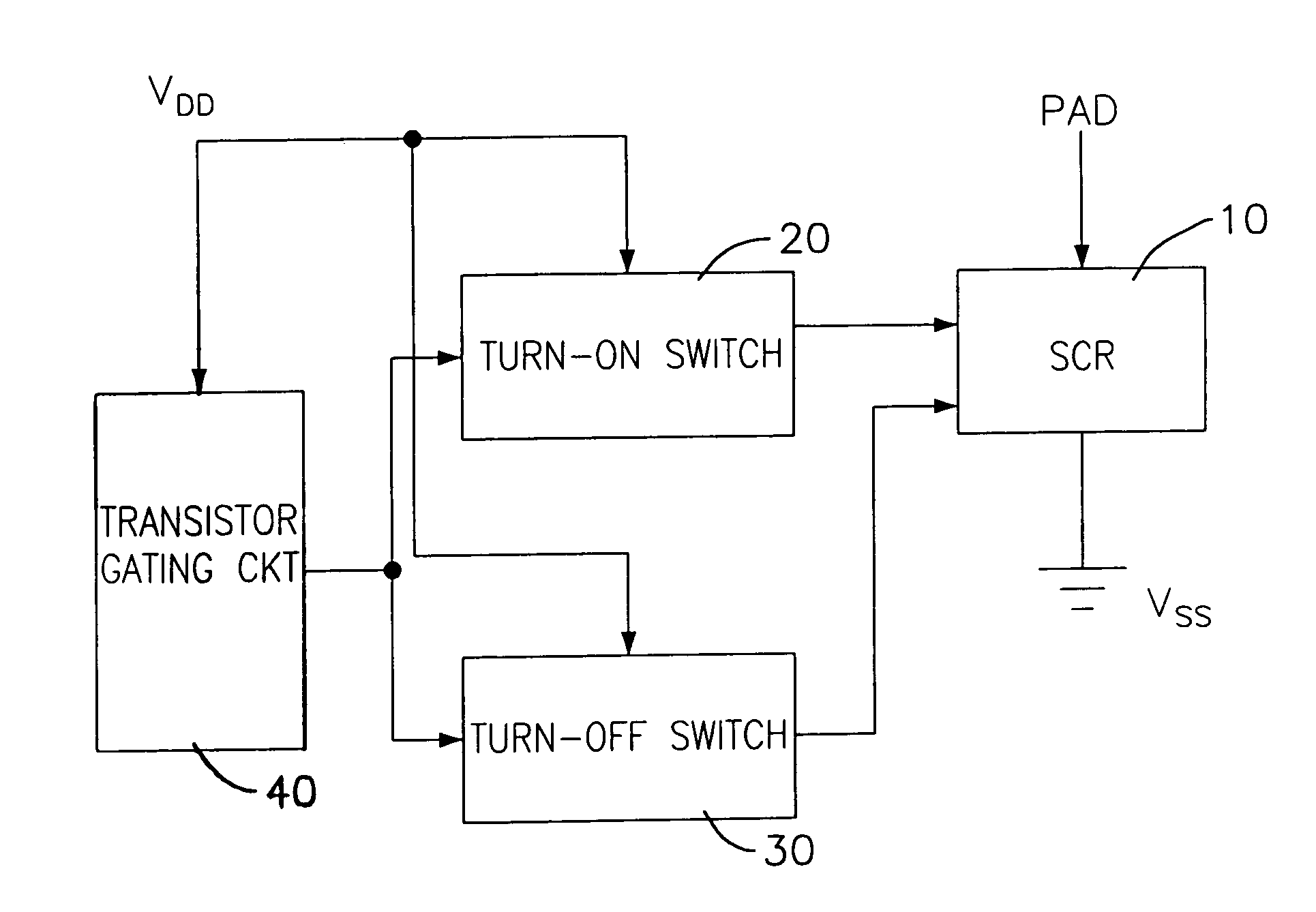
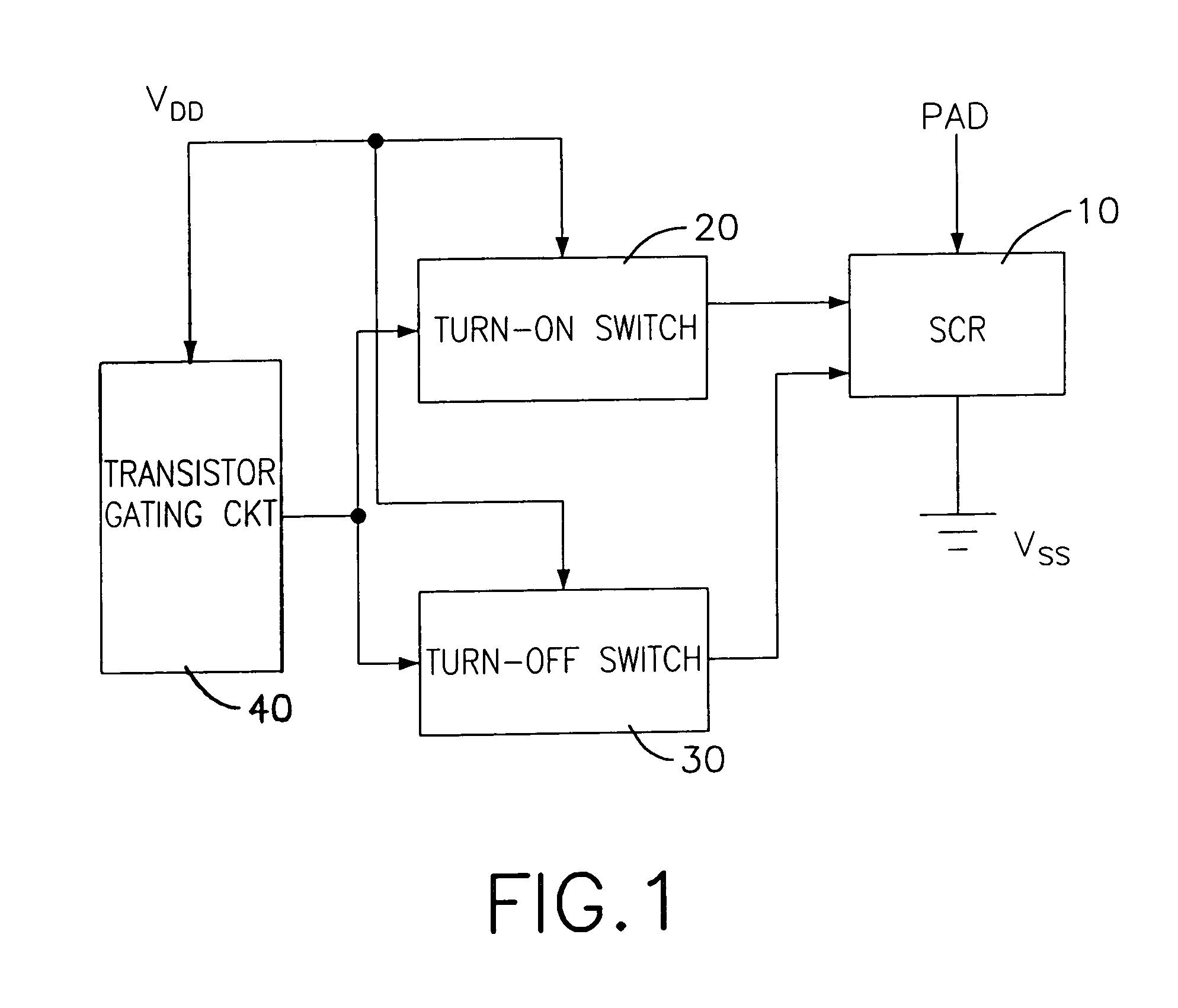
[0064]In the fourth embodiment, the SCR (10) as shown in FIG. 5, is formed by a PNP transistor (11) and an NPN transistor (12), both being bipolar junction transistors. The emitter of the PNP transistor (11) forms an anode of the SCR (10), and the base through a resistor RN is connected to the anode, and the collector of the PNP transistor (11) is connected to the base of the NPN transistor (12), and through a resistor RSUB is connected to the negative power supply VSS to form a cathode of the SCR (10). The emitter of the NPN transistor (12) is coupled with a diode D1, forming another cathode of the SCR (10). The bases of the PNP transistor and the NPN transistor act as the gate of the SCR (10).

[0065]The turn-on switch (20) is formed by an NMOS (21) and a voltage clamping circuit (22), wherein the drain of the NMOS (21) is connected to the base of the PNP transistor (11) of the SCR (10), and the gate is connected to the transistor gating circuit (40) to enable the SCR (10). The volt...

fifth embodiment

[0073]ESD protection circuit as shown in FIG. 6 employs an NMOS (14) to replace the diode D1 of the SCR (10).

[0074]When forward overvoltage stress develops, the transistor gating circuit (40) produces a high voltage pulse and a forward voltage is generated to cause the NMOS (14) in the turn-on switch (20) to be turned on. The function of the NMOS (14) is similar to that of PMOS (13) shown in FIG. 4, wherein the NMOS (14) is connected to the emitter of the PNP transistor (11). Since the voltage drop through the NMOS (14) is below the trigger voltage of the diode, when the SCR (10) remains in conduction, and the holding voltage is lowered, better protection can be achieved in electrostatic discharge.

[0075]According to the present invention, the SCR (10) is able to provide effective ESD protection, irrespective whether the overvoltage stress is developed in the fast-transient or quasi-static mode.

[0076]In conclusion, the present invention provides a technique to trigger an SCR into con...


PUM


Abstract

A latch-up-free ESD protection circuit using SCR is disclosed, in which an SCR is connected between the input pad and the negative power supply; a turn-on switch and a turn-off switch are connected between the positive power supply VDD (or the input pad) and the SCR; and a transistor gating circuit is connected to the turn-on switch and the turn-off switch to direct the operation of the SCR. When overvoltage stress develops over the input pad in the fast-transient mode, the turn-on switch enables the NPN transistor to switch on the SCR to form a discharging path for electrostatic discharge; and when overvoltage stress is released, the turn-off switch enables the PNP transistor to switch off the SCR, thus making it immune to any latch-up after the overvoltage stress is released, and having the advantages of fast triggering, low trigger voltage, no latch-up, and full ESD protection in the active and passive modes.

Description

BACKGROUND OF THE INVENTION[0001]1. Field of the Invention[0002]The present invention is related to a latch-up-free ESD protection circuit using an silicon controlled rectifier (SCR), and more particularly to an ESD protection circuit that employs a turn-on switch to turn on an SCR and a turn-off switch to switch off the SCR, whereby plural discharging paths are formed even after another part of the SCR is switched off.[0003]2. Description of Related Art[0004]When an operator touches a semiconductor device, the electrostatic charge stored on the surface of human body is transferred to the device with a burst of high voltage electrostatic charge, thus causing destructive damage to the device. Therefore, an ESD protection circuit is important to the reliable operation of any semiconductor device.[0005]Two ESD protection schemes have been used. The first type of conventional ESD protection circuit employs a pair of gate-insulated MOSFET devices, and can be either a thick-oxide or a thi...

Claims


Application Information

Patent Timeline
Patent Type & Authority Patents(United States)
IPC IPC(8): H02H9/00H01L27/02
CPCH01L27/0262
Inventor LIU, JAMESHSIEH, JIMMYJANG, SHENG-LYANGLU, HSUEH-MING
Owner KING BILLION ELECTRONICS
Why Eureka
Try Eureka