Image forming apparatus using a contact or a proximity type of charging system including a protection substance on a moveable body to be charged

a technology of contact or proximity and image forming apparatus, which is applied in the direction of electrographic process apparatus, corona discharge, instruments, etc., can solve the problems of discharge chemically deteriorating the surface of the charged body, irregular discharge, and irregular discharg

Active Publication Date: 2006-09-05
RICOH KK
View PDF81 Cites 47 Cited by
  • Summary
  • Abstract
  • Description
  • Claims
  • Application Information

AI Technical Summary

Benefits of technology

[0015]It is therefore an object of the present invention to provide a small-size image forming apparatus using a contact or a proximity type of charging system and capable of protecting the surface of a body to be charged from chemical deterioration, a charger and a cleaning device for use in the image forming apparatus, and a process cartridge.

Problems solved by technology

Corona discharge, however, produces ozone, NOx (nitrogen oxides) and other discharge products that are apt to form a nitric acid film or a nitrate film having adverse influence on an image on the surface of the image carrier.
However, a problem with the contact or the proximity type of charging system is that discharge occurs toward the body to be charged either directly or via a small gap, resulting in irregular discharge and therefore irregular charging.
However, this system brings about another problem that the discharge chemically deteriorates the surface of the body charged.
Such chemical deterioration, e.g., shaving of the film thickness of the photoconductive layer occurs even when mechanical rubbing is absent.
Such chemical deterioration reduces the thickness of a charge transport layer (CTL) positioned on the surface of the photoconductive element little by little, causing inorganic fine grains contained in the CTL to separate and part.
If the inorganic fine grains thus parted deposit on a cleaning member or similar member contacting the photoconductive element, then they constitute abrasive grains and therefore cause the surface of the element to locally wear, e.g., shaves off the surface in the form of stripes.
Particularly, the AC-biased DC voltage generates discharge having greater energy than a DC voltage, aggravating the deterioration.
Further, when the shave-off of the photoconductive layer proceeds, it is more likely that the charge potential of the photoconductive element drops, the photoconductive element is deteriorated, background is contaminated due to, e.g., scratches formed on the surface of the element, image density decreases, and image quality is lowered.
Such schemes, however, are not always successful to obviate the chemical deterioration ascribable to proximity type of charging although they may improve wear resistance.
However, the means taught in these documents are configured to reduce the coefficient of friction of the surface in order to obviate toner filming, toner melting and defective cleaning.
The above documents therefore do not address to the protection of the surface of a photoconductive element from deterioration ascribable to discharge.
Moreover, zinc stearate, simply coated to reduce the coefficient of friction, cannot always obviate deterioration ascribable to discharge.
More specifically, the schemes taught in Laid-Open Publication Nos. 2002-55580 and 2002-244487 mentioned above are likely to fail to protect, in the contact or the proximity type of charging system, the surface of the photoconductive element from chemical deterioration conspicuous with discharge caused by an AC voltage (AC discharge hereinafter).

Method used


Image

  • Image forming apparatus using a contact or a proximity type of charging system including a protection substance on a moveable body to be charged
  • Image forming apparatus using a contact or a proximity type of charging system including a protection substance on a moveable body to be charged
  • Image forming apparatus using a contact or a proximity type of charging system including a protection substance on a moveable body to be charged

Examples


first embodiment

[0070]First, why the illustrative embodiment can achieve the object of the present invention stated earlier will be described on the basis of the results of various experiments.

Experiment 1

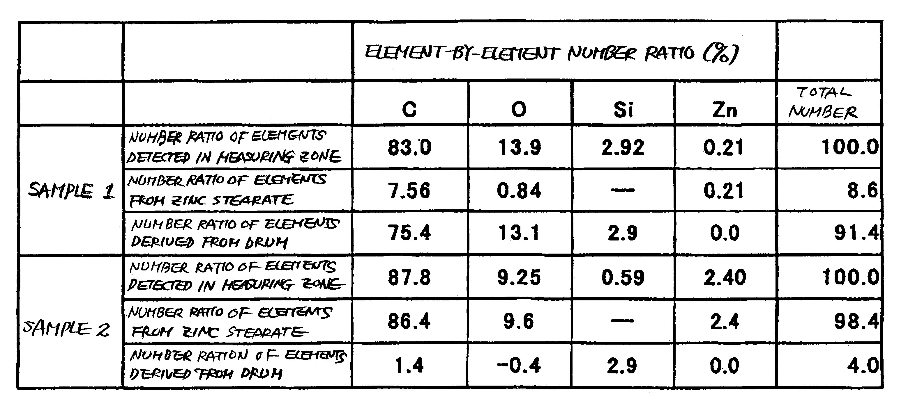
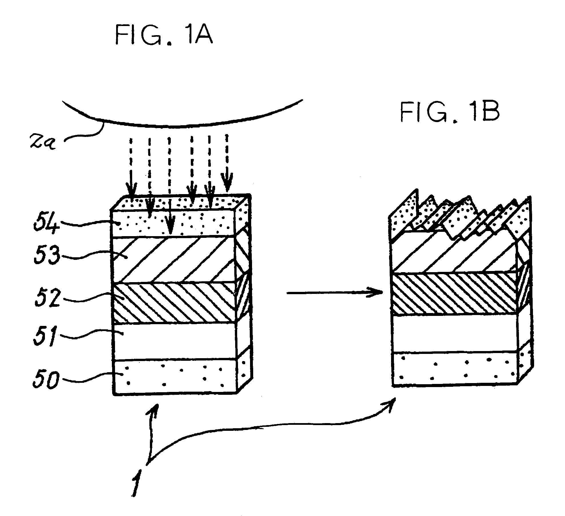
[0071]We conducted the following experiment in order to examine the deterioration of the surface of a photoconductive element or body to be charged that is conspicuous with a charging member contacting or adjoining the photoconductive element and applied with an AC bias. As shown in FIG. 1A, a charging member, implemented as a rotatable roller-like charging member (charge roller hereinafter), 2a was spaced from the surface of a photoconductive element 1 in order to exclude deterioration ascribable to mechanical wear and was applied with an AC-biased DC voltage. The charge roller 2a was caused to continuously charge the photoconductive element 1 for about 150 hours.

[0072]As shown in FIG. 1A, the photoconductive element 1 included a base layer 50 and an under layer or insulation layer 51 formed on t...

experiment 4

[0095]Hereinafter will be described an experiment showing that the amount of shaving is proportional to the peak-to-peak voltage Vpp of the AC voltage, i.e., the amplitude of the AC component applied to the charge roller 2a. For the experiment, the arrangement of the photoconductive element 1, charger 2 and coating device 30 shown in FIG. 3A was used. To obviate the deterioration of the surface ascribable to mechanical wear, all members other than the charge roller 2 and coating device 30 were removed. The surface of the photoconductive element 1 was continuously charged for 100 hours by discharge using an AC voltage whose Vpp was varied. The experiment was conducted under the following conditions:

[0096]Charging Conditions:[0097]Vpp=2.2, 2.6 and 3.0 kV[0098]f=−600 V[0099]moving speed v=113 mm / sec

[0100]Protection Substance: Zinc Stearate

[0101]Charging Time: 100 hours

[0102]FIG. 7 plots the amounts of shaving determined after continuous 100 hours of discharge with respect to Vpp. As sh...

experiment 5

[0104]An experiment showing that the shaving of the surface of the photoconductive element 1, conspicuous with AC discharge, is proportional to the frequency f of the AC voltage will be described hereinafter. Experiment 5 is identical with Experiment 4 as to the basic configuration and experimental conditions except for the charging conditions and moving speed. More specifically, while Experiment 4 varies Vpp while fixing the frequency f of the AC voltage, Experiment 5 varies the frequency f while fixing Vpp.

[0105]Experimental conditions are as follows.

[0106]Charging Conditions:[0107]Vpp=2.2 kV[0108]f=500, 900, 1,400, 2,000 and 4,000 Hz[0109]DC voltage=−600 V[0110]moving speed=104 mm / sec

[0111]Protection Substance: zinc stearate

[0112]Charging Time: 100 hours

[0113]FIG. 8 plots the amounts of shaving of the surface after 100 hours of charging effected by the above discharge with respect to the frequency f. As shown, the amount of saving is proportional to the frequency f.

[0114]The resu...


PUM


Abstract

An image forming apparatus of the present invention includes a movable body to be charged and a charger including a charging member that contacts or adjoins the body to be charged and applies a voltage, including an AC component, to the charging member for thereby charging the body. A protection substance for protecting the surface of the body from deterioration ascribable to charging is caused to exist on the body. The number of particular elements, contained in the protection substance and detected by an X-ray photon spectral analyzer (XPS) in a zone where the charging member charges the body, is held in a particular ratio to the total number of all elements constituting the outermost surface of the body and also detected by the XPS.

Description

DESCRIPTION OF THE BACKGROUND ART[0001]1. Field of the Invention[0002]The present invention relates to a copier, facsimile apparatus, printer or similar image forming apparatus and more particularly to a contact or a proximity type of charger and a cleaning device included in the image forming apparatus.[0003]2. Description of the Background Art[0004]Generally, an electrophotographic image forming apparatus includes various charging means, e.g., one for uniformly charging the surface of a photoconductive element or image carrier before the formation of a latent image, one for quenching the charged surface of the image carrier after image transfer, and one for charging a sheet or recording medium conveyed to an image transfer position. Such charging means have customarily been implemented by a corona discharge type of charging system. In this type of charging system, a charge wire is positioned in the vicinity of a body to be charged and applied with a high voltage, so that corona di...

Claims


Application Information

Patent Timeline
Patent Type & Authority Patents(United States)
IPC IPC(8): G03G15/00G03G15/02
CPCG03G15/0208G03G15/0216G03G15/025G03G15/751G03G2215/00957G03G2221/0005
Inventor WATANABE, KAZUHIKOWATANABE, KAZUHITOSUZUKI, YASUOTAMOTO, NOZOMUNAKAI, HIROSHITOKUMASU, TAKAHIKOOHSHIMA, KOHICHIMATSUURA, NEKKA
Owner RICOH KK
Why Eureka
Try Eureka