EMI shielding for electronic component packaging

Inactive Publication Date: 2006-09-19
WAVEZERO +1
View PDF19 Cites 73 Cited by
  • Summary
  • Abstract
  • Description
  • Claims
  • Application Information

AI Technical Summary

Benefits of technology

[0019]The conductively coated polymer shield may be used to create a spacing between the conformal coating and the die. Such a spacing may reduce the mechanical stress and thermal mismatch stress between the die and conformal coating. Optionally, a filler material may be positioned within the spacing adjacent the die. The filler material may have a coefficient of thermal expansion that is similar to the coefficient of thermal expansion of the electronic die that it encapsulates. Alternatively, the filler material may have a coefficient of thermal expansion that is higher or lower than the die, (

Problems solved by technology

The problem of emittance of electromagnetic radiation is not new to designers of electronic equipment.
Unfortunately, one problem associated with conventional packaging of the semiconductor electronic component is that such thermoplastic package does not provide shielding from electromagnetic radiation, such as RFI and EMI.
However, as the frequency of chips increase (e.g., greater than 3 GHz) and the data transmission rates increase, the creation of errant EMI radiation becomes much easier and more harmful to adjacent circuits and components.
Thus, in general, conventional solutions will increasingly find themselves inadequate for purposes of immunity and indeed, radiate

Method used


Image

  • EMI shielding for electronic component packaging
  • EMI shielding for electronic component packaging
  • EMI shielding for electronic component packaging

Examples


Embodiment Construction

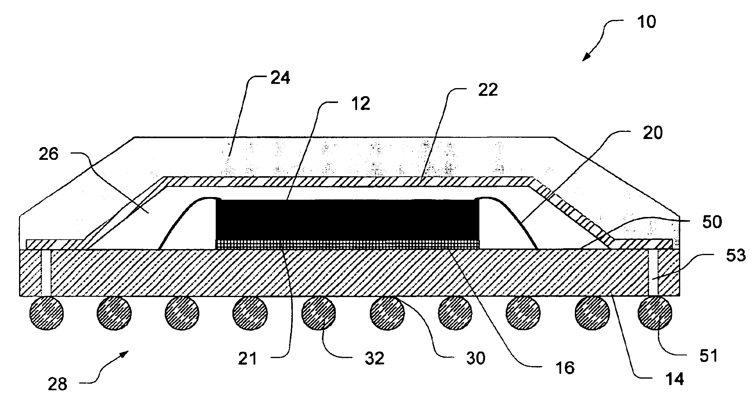
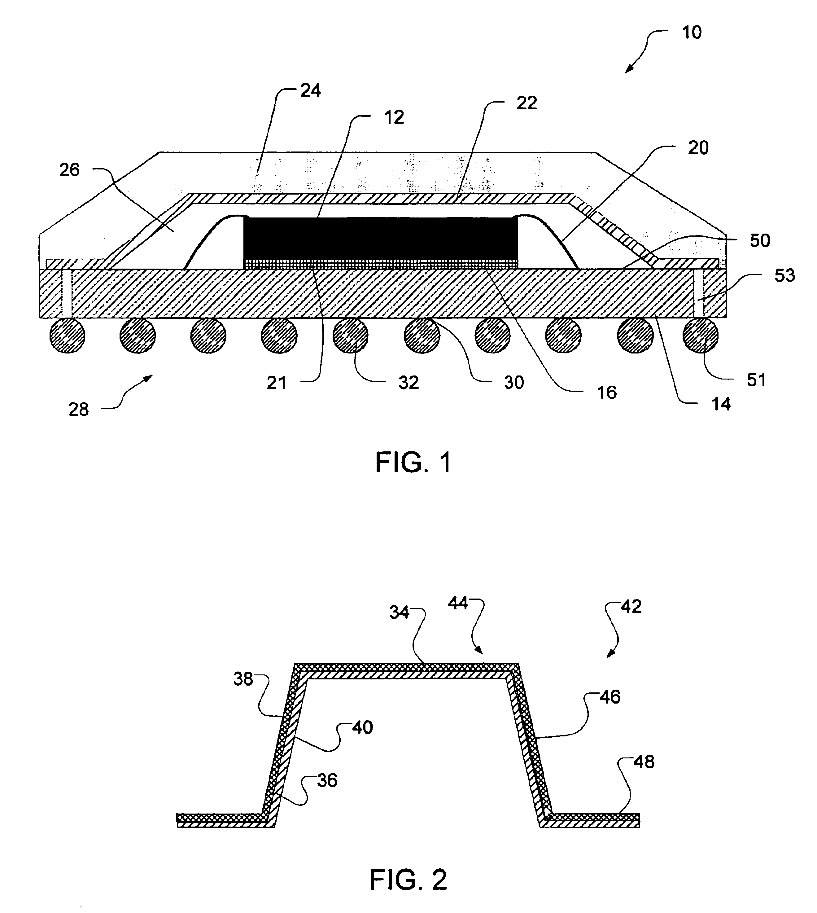
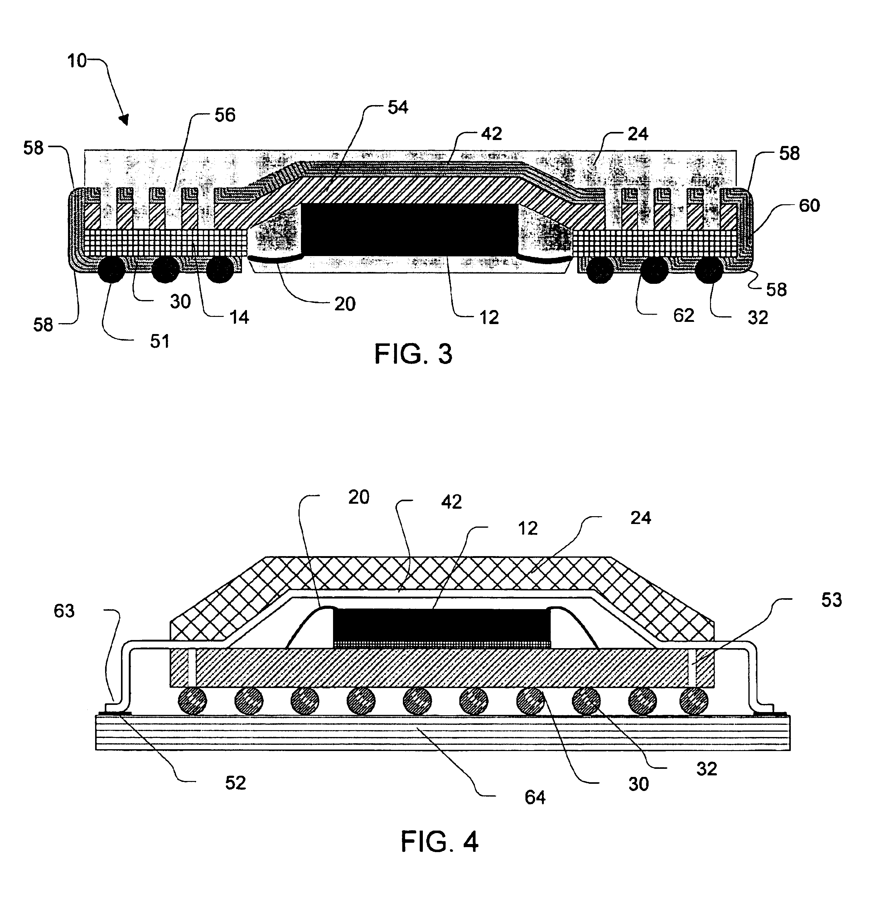
[0038]FIG. 1 illustrates one electronic package 10 that is encompassed by the present invention. The package 10 comprises a die 12 positioned on a die pad of a substrate 14. Die 12 is typically coupled to the die pad with an adhesive layer 16. The die is electrically coupled to conductive traces (not shown) on the substrate 14 with a plurality of conductive elements 20 such as an array of wires or an array of solder balls. If the conductive elements 20 are solder balls, such solder balls will typically be disposed on an underside 21 (which would be the active face) of the die and may be used to attach die 12 to the traces of substrate 14. In such an embodiment, the adhesive 16 is typically not necessary, but a non-conductive adhesive or other material may be used to insulated conductive elements from each other and to provide mechanical support for the die.

[0039]A spacing element insert 22 may be positioned over die 12 and be coupled to a portion of substrate 14. A conformal coating...


PUM


Abstract

The present invention provides methods and devices for shielding an electronic component package. In one embodiment, an EMI shield is integrally formed within the package adjacent the die and grounded. The EMI shield may be a metallized shaped polymer layer and may be disposed fully within the package or it may extend out of the package.

Description

CROSS-REFERENCES TO RELATED APPLICATIONS[0001]The present application claims benefit to provisional U.S. patent application Ser. No. 60 / 462,902, filed Apr. 15, 2003, the complete disclosure of which is incorporated herein by reference.[0002]The present application is also related to co-pending and commonly owned U.S. patent application Ser. No. 10 / 825,999, entitled “Electromagnetic Interference Shielding for a Printed Circuit Board”, filed herewith, the complete disclosure of which is also incorporated herein by reference.BACKGROUND OF THE INVENTION[0003]The present invention generally provides shielded semiconductor electronic packages and printed circuit boards. More specifically, the present invention provides an EMI shield integrally formed within a package of a semiconductor electronic component.[0004]Semiconductor electronic components emit electromagnetic radiation, generally in the range of 50 MHz to 3 GHz, depending on the speed of the microprocessor. As can be appreciated,...

Claims


Application Information

Patent Timeline
IPC IPC(8): H05K9/00H01L23/04H01L23/31H01L23/433H01L23/485H01L23/49H01L23/498H01L23/50H01L23/552H05K1/02H05K3/34
CPCH01L23/04H01L23/3128H01L23/315H01L23/4334H01L23/49816H01L23/49822H01L23/49838H01L23/50H01L23/552H01L24/49H05K1/0218H05K3/3484H01L21/50H01L24/16H01L24/48H01L2224/16H01L2224/48091H01L2224/48227H01L2224/49171H01L2224/49175H01L2224/73253H01L2924/01006H01L2924/01013H01L2924/01014H01L2924/01027H01L2924/01028H01L2924/01029H01L2924/01033H01L2924/01047H01L2924/0105H01L2924/01074H01L2924/01078H01L2924/01079H01L2924/01082H01L2924/14H01L2924/15192H01L2924/15311H01L2924/1532H01L2924/16152H01L2924/1617H01L2924/16315H01L2924/166H01L2924/3011H01L2924/3025H05K2201/10734H01L2924/014H01L2224/48233H01L2224/32225H01L2224/73265H01L2924/07802H01L2224/16235H01L2924/00014H01L2924/00H01L2924/181H05K9/003H01L2924/12042H05K9/0035H01L2224/45099H01L2224/05599
Inventor ARNOLD, ROCKY R.ZARGANIS, JOHN C.MONTAUTI, FABRIZIO
Owner WAVEZERO
Why Eureka
Try Eureka