SOI substrate, element substrate, semiconductor device, electro-optical apparatus, electronic equipment, method of manufacturing the SOI substrate, method of manufacturing the element substrate, and method of manufacturing the electro-optical apparatus

a technology of soi substrate and element substrate, which is applied in the field of soi substrate, can solve the problems of deterioration in element property, difficult or impossible to perfectly prevent atmospheric impurities from being absorbed onto the lamination surface, and fear of element property deterioration

Inactive Publication Date: 2006-09-26
SEIKO EPSON CORP
View PDF7 Cites 60 Cited by
  • Summary
  • Abstract
  • Description
  • Claims
  • Application Information

AI Technical Summary

Benefits of technology

[0019]The present invention is proposed in view of the above-mentioned circumstances. Firstly, it is therefore an object of the present invention to provide an SOI substrate, which can almost perfectly prevent impurities contained in a support substrate or impurities absorbed on a lamination plane between the support substrate and a single crystal silicon substrate from being diffused into a side of a single crystal silicon layer, and a method of manufacturing the same.

Problems solved by technology

This results in the fear of the deterioration in the element property.
Actually, even if the dust-proof filter is used, it is difficult or impossible to perfectly prevent the atmospheric impurities from being absorbed onto the lamination surface.
Secondly, for example, in a case of an electro-optical apparatus of a TFT active matrix driving type, if an input light is irradiated onto a channel region of a thin film transistor (hereafter, which is referred to as a TFT (Thin Film Transistor) as the occasion demands) for a pixel switching operation, which is disposed at each pixel, an optical excitation causes an optical leak current to be generated, which changes the TFT property.
However, according to the research of the inventor of this application, the light shield film, which is formed at the lower side of the TFT and is made of the metal of the high melting point and the like, exhibits the tendency of the increase in aging oxidation during the manufacture of a product or the usage after the completion of the product.
This results in a problem that the increase in the oxidation causes the original function of the light shield film to be not sufficiently provided.
Moreover, according to the research of the inventor of this application, the above-mentioned arrangement of the light shield film made of the high melting point metal and the like at the lower side of the channel region of the semiconductor layer constituting the TFT results in a problem of the contamination caused by the light shield film in this semiconductor layer (e.g., the contamination caused by the diffusion of the impurities and the like).
That is, as compared with the case in which such a light shield film is not disposed, the example of the increase in the impurities permeated into the semiconductor layer is also confirmed, which results in a problem of the deterioration in the transistor property of the TFT.

Method used


Image

  • SOI substrate, element substrate, semiconductor device, electro-optical apparatus, electronic equipment, method of manufacturing the SOI substrate, method of manufacturing the element substrate, and method of manufacturing the electro-optical apparatus
  • SOI substrate, element substrate, semiconductor device, electro-optical apparatus, electronic equipment, method of manufacturing the SOI substrate, method of manufacturing the element substrate, and method of manufacturing the electro-optical apparatus
  • SOI substrate, element substrate, semiconductor device, electro-optical apparatus, electronic equipment, method of manufacturing the SOI substrate, method of manufacturing the element substrate, and method of manufacturing the electro-optical apparatus

Examples


Embodiment Construction

[0140]Preferred embodiments of the present invention will be explained below with reference to the accompanying drawings. In the following embodiments, an electro-optical apparatus of the present invention is applied to a liquid crystal display device of a TFT active matrix driving type.

(SOI Substrate)

[0141]First of all, an embodiment of an SOI substrate of the present invention is described.

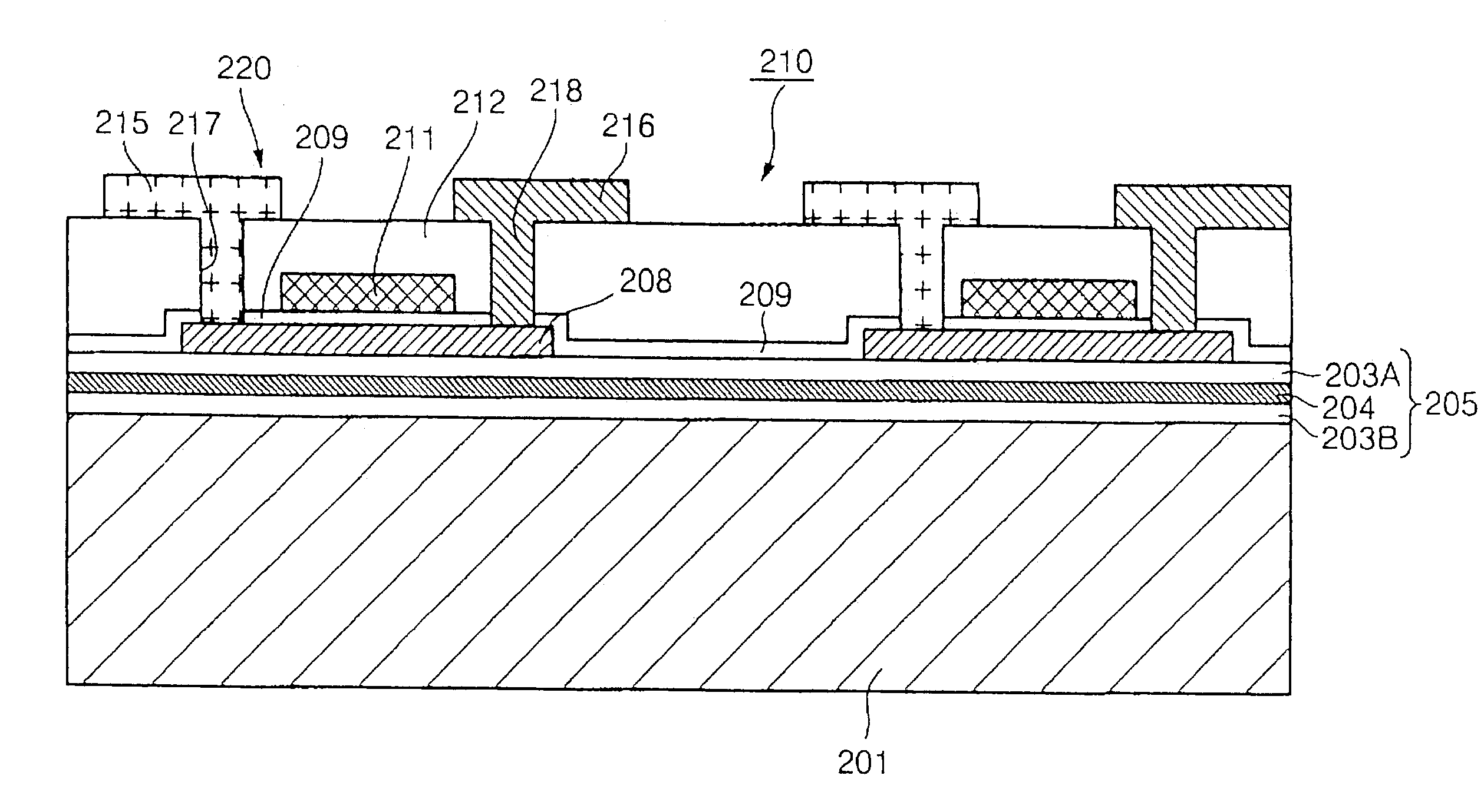
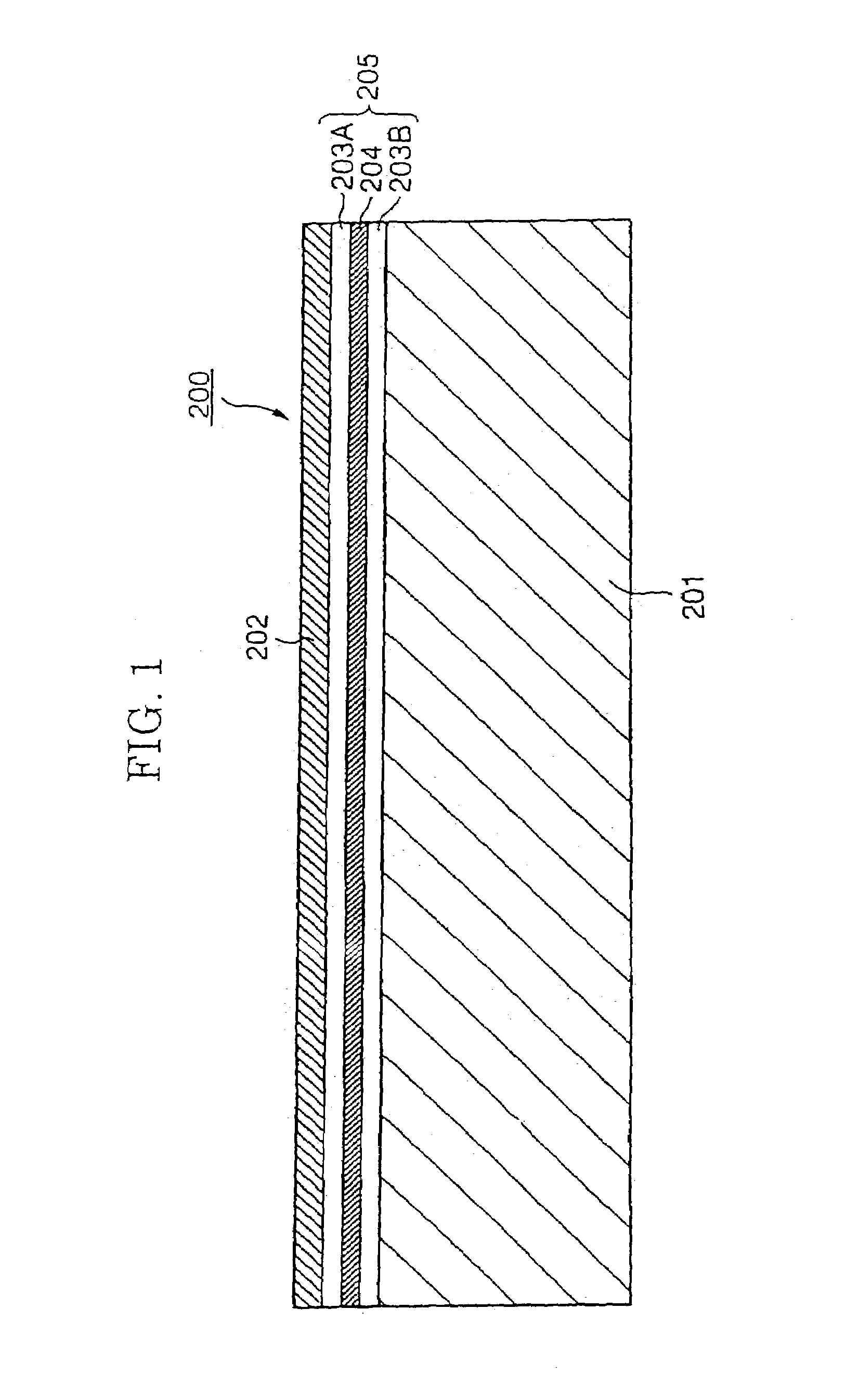
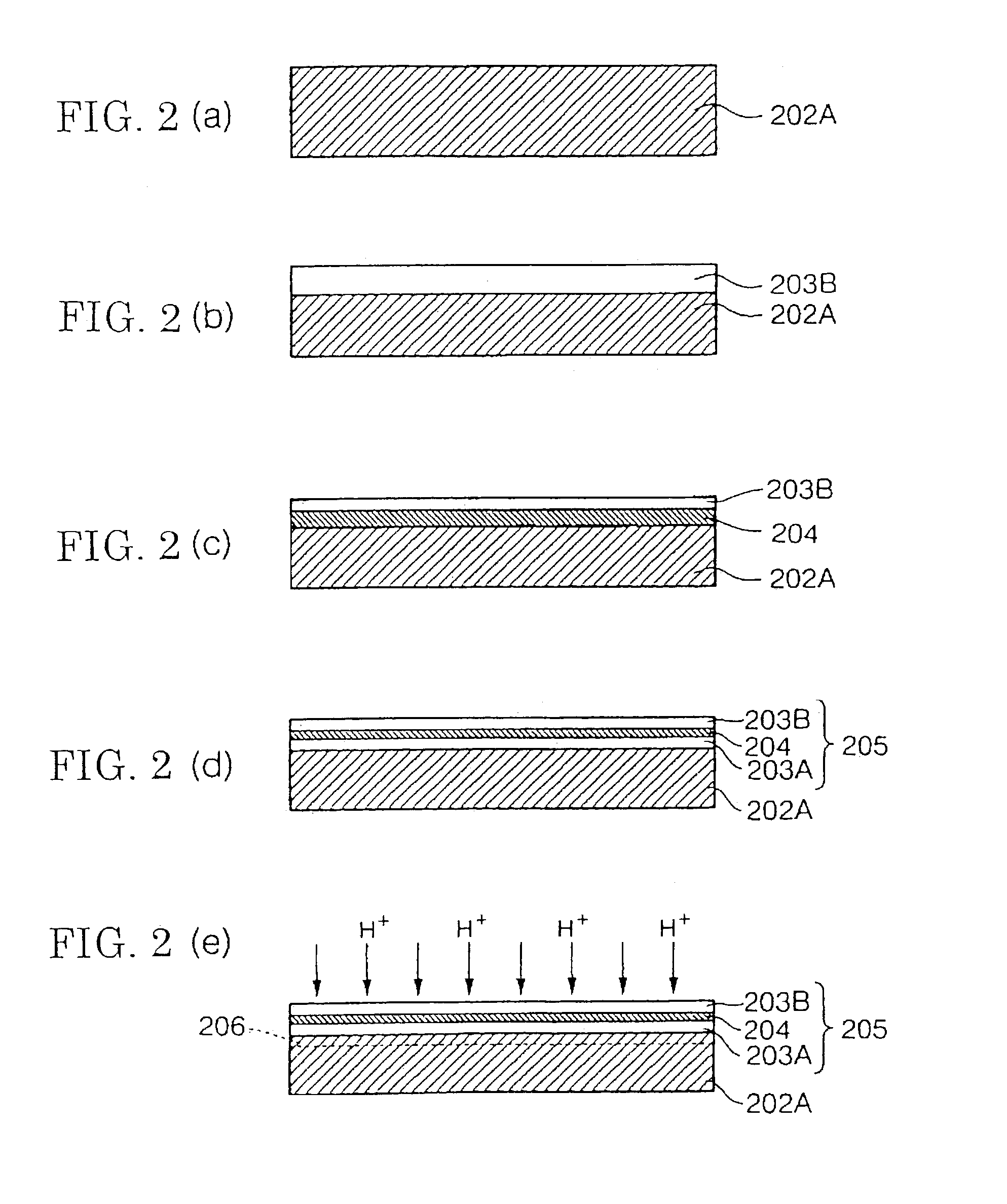
[0142]At first, FIG. 1 shows the sectional structure of the SOI substrate in this embodiment. This structure of an SOI substrate 200 is described.

[0143]As shown in FIG. 1, the SOI substrate 200 in this embodiment is provided with: a support substrate 201 made of silicon, quartz, glass or the like; and a single crystal silicon layer 202. An insulation portion 205 having a lamination structure including a plurality of insulation films is formed between the support substrate 201 and the single crystal silicon layer 202. In this embodiment, the insulation portion 205 is configured such that a first ...


PUM

PropertyMeasurementUnit
thicknessaaaaaaaaaa
thicknessaaaaaaaaaa
thicknessaaaaaaaaaa

Abstract

An SOI (Silicon On Insulator) substrate is provided with: a support substrate (201); a single crystal silicon layer (202) disposed above one surface of the support substrate; an insulation portion (205) disposed between the support substrate and the single crystal silicon layer, the insulation portion comprising a single layer of an insulation film or a lamination structure of a plurality of insulation films, and including a silicon nitride film or a silicon nitride oxide film (204).

Description

[0001]This is a Division of Application Ser. No. 09 / 988,332 filed Nov. 19, 2001 now U.S. Pat. No. 6,583,440. The entire disclosure of the prior application is hereby incorporated by reference herein in its entirety.BACKGROUND OF THE INVENTION[0002]1. Field of the Invention[0003]The present invention relates to an SOI (Silicon On Insulator) substrate having a single crystal silicon layer on one surface of a support substrate, an element substrate having the SOI substrate, a semiconductor device having the SOI substrate, an electro-optical apparatus having the element substrate, an electronic equipment, a method of manufacturing the SOI substrate, a method of manufacturing the element substrate, and a method of manufacturing the electro-optical apparatus.[0004]2. Description of the Related Art[0005]At first, a semiconductor technique for forming a single crystal silicon thin film on an insulation substrate and, by using the single crystal silicon thin film, forming a semiconductor dev...

Claims


Application Information

Patent Timeline
Patent Type & Authority Patents(United States)
IPC IPC(8): H01L21/30H01L21/762H01L21/77H01L21/84H01L27/12H01L29/786
CPCH01L21/76254H01L27/1203H01L27/1214H01L27/1266H01L27/1218H01L29/78633H01L29/78603H01L2221/68359H01L2221/68363Y10S438/977H01L27/12
Inventor YASUKAWA, MASAHIRO
Owner SEIKO EPSON CORP
Why Eureka
Try Eureka