Liquid crystal process defect inspection apparatus and inspection method

a liquid crystal and process defect technology, applied in the field of lcd manufacturing, can solve the problems of inability to detect kind of stain, different luminance distributions of stains from other areas, and inconsistent anisotropy on alignment layers, etc., and achieve the effect of 100% yield

Inactive Publication Date: 2006-09-26
SAMSUNG DISPLAY CO LTD
View PDF4 Cites 6 Cited by
  • Summary
  • Abstract
  • Description
  • Claims
  • Application Information

AI Technical Summary

Benefits of technology

[0018]It is an object of the present invention to provide a glass substrate test apparatus and method for optically inspecting defects of an alignment layer immediately after each unit process so as to secure a 100% yield in the liquid crystal cell process.

Problems solved by technology

However, componential anisotropy can exist on the alignment layer, caused by remaining solvent that does not evaporate because of a difference in curing speed even though the surface of the alignment layer appears even.
The componential anisotropy of the alignment layer generates electrostatic alignment anisotropy when charging the liquid crystal material so as to locally destroy alignment on the alignment layer, resulting in stains having different luminance distributions from other areas.
In the conventional inspection method, this kind of stain cannot be detected immediately after the alignment layer cure process.
If the stain is detected after the liquid crystal is charged, it is impossible to rework the glass substrate so the yield cannot be improved.
In the alignment layer rubbing process, since uniform furrows having a depth of 50˜60 Å are formed, it is impossible to detect defects immediately after the rubbing, but rather an insufficiency of alignment can only be detected by an electrostatic correlation of the rubbing direction and the liquid crystal after the liquid crystal is charged into the liquid crystal cell.
Accordingly, in this method, rubbing rework is impossible, and even though the defects are detected, it does not help in improving the yield.

Method used


Image

  • Liquid crystal process defect inspection apparatus and inspection method
  • Liquid crystal process defect inspection apparatus and inspection method
  • Liquid crystal process defect inspection apparatus and inspection method

Examples


Embodiment Construction

[0047]A preferred embodiment of the present invention will be described hereinafter with reference to the accompanying drawings.

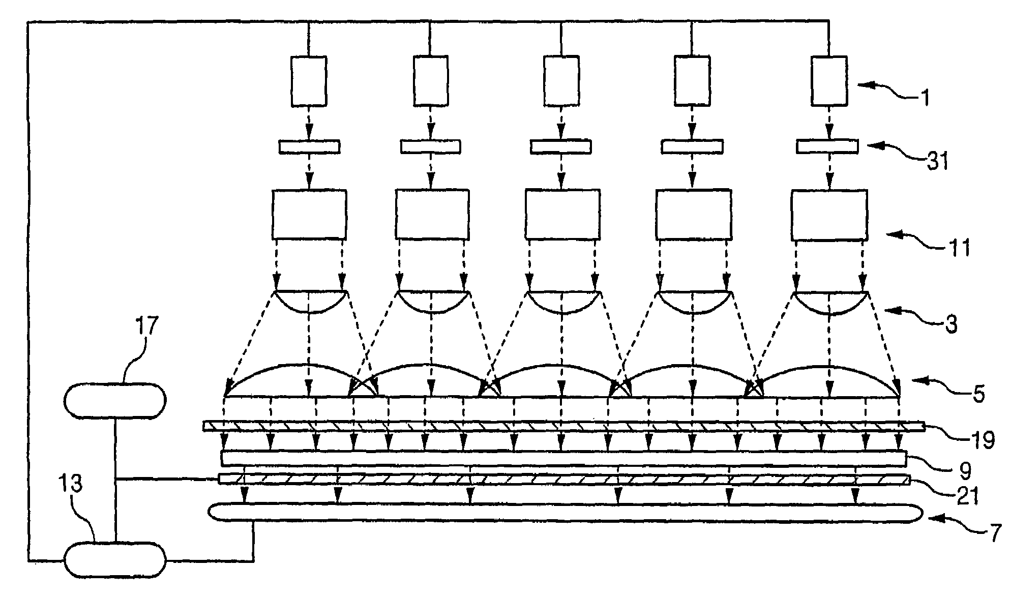
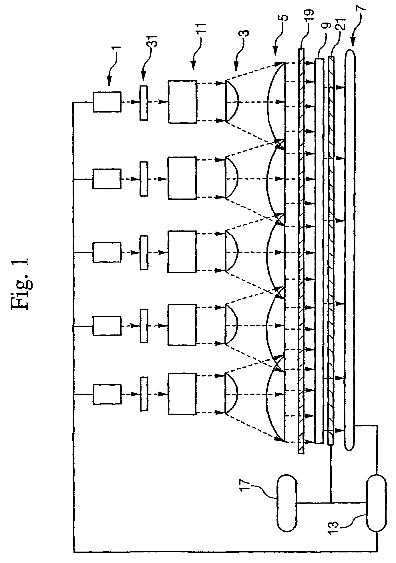
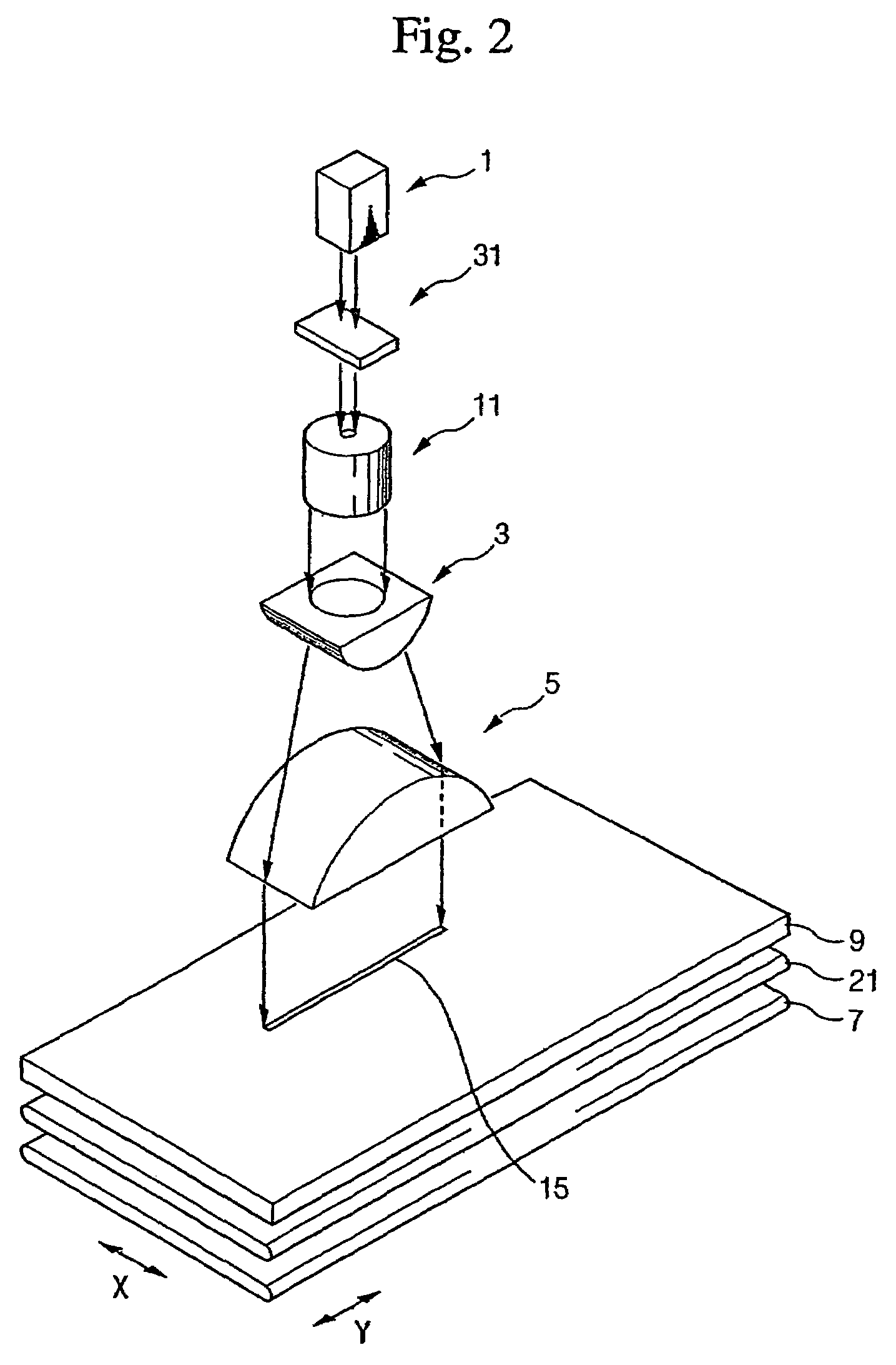
[0048]FIG. 1 is a schematic view showing an apparatus for testing a glass substrate immediately after depositing an alignment layer and / or rubbing the surface of the alignment layer.

[0049]In FIG. 1, laser beams are projected to the alignment layer of the glass substrate passing below the laser unit such that the anisotropy of the double refraction of the laser beam caused by the characteristics of the alignment layer is measured so as to be collected as data for determining whether or not the glass substrate has defects.

[0050]The laser beam emitted from the laser unit is shaped through an optical system and the shaped laser beam scans the surface of the glass substrate for measuring the double refraction such that it is determined whether or not the glass substrate is defective by comparing the measured double refraction data to a standard double refraction...


PUM

PropertyMeasurementUnit
wavelengthsaaaaaaaaaa
oscillation wavelengthaaaaaaaaaa

Abstract

The glass substrate test apparatus of the liquid crystal cell process comprises a laser unit for generating a laser beam, a beam shaper and beam collimator for shaping the laser beam emitted from the laser unit so as to have an elongated cross section and parallelizing the shaped laser beam, a photo detector for detecting an intensity of double refraction of the shaped laser beam transmitted over the whole glass substrate, a phase defector for measuring the laser double refraction detected by the photo detector and comparing the measured double refraction with a standard laser double refraction, and a polarizer arranged between the laser unit and the beam shaper or between the beam shaper and the beam collimator for polarizing the laser beam to a parallel ray.

Description

BACKGROUND OF THE INVENTION[0001](a) Field of the Invention[0002]The present invention relates to LCD manufacturing, and in particular, to a glass substrate test apparatus and method for optically inspecting defects of an alignment layer before charging liquid crystal into a liquid crystal cell.[0003](b) Description of the Related Art[0004]Typically, LCD manufacturing includes thin film transistor (TFT) array fabrication, color filter fabrication, and liquid crystal cell fabrication processes.[0005]The TFT fabrication process is similar to the process used to fabricate semiconductor devices where various steps are repeatedly performed, such that it is possible to control a yield by making a decision on proceeding to a next process or reworking the same process by capturing defects immediately after each unit process.[0006]That is, since the basic TFT fabrication process includes the steps of depositing metal and organic material layers and patterning the same, it is possible to insp...

Claims


Application Information

Patent Timeline
Patent Type & Authority Patents(United States)
IPC IPC(8): G01J4/00G01N21/23G02F1/13G01N21/896G01N21/958
CPCG01N21/896G01N21/23G02F1/13
Inventor CHOO, DAE-HOWON, MIN-YOUNGNAM, HYOO-HAKJEON, BEAK-KEUN
Owner SAMSUNG DISPLAY CO LTD
Why Eureka
Try Eureka