Method and system for reducing power consumption in digital circuitry using charge redistribution circuits

a technology of digital circuitry and charge redistribution circuit, which is applied in the direction of power consumption reduction, pulse technique, instruments, etc., can solve the problems of increasing the concern the limiting factor of transistor drive capability, and the increase of power consumption and dissipation concerns, etc., to achieve the effect of reducing power consumption in digital circuits

Active Publication Date: 2006-10-03
STMICROELECTRONICS PVT LTD
View PDF3 Cites 21 Cited by
  • Summary
  • Abstract
  • Description
  • Claims
  • Application Information

AI Technical Summary

Benefits of technology

[0006]To address the above-discussed deficiencies of the prior art, a primary object of this invention is to pro

Problems solved by technology

However, even though power supply voltage has been lowered considerably, the combination of size and transistor count is such that chip power consumption continues to grow resulting in increased concern with power consumption and dissipation.
Power consumption and dissipation concerns have become a limiting factor in the design of LSIs used in microprocessors and other devices that require large-scale, high-speed processing.
Attempts to limit power consumption while reducing power source voltage that have been made so far have however resulted in a decline in transistor drive capability resulting in re

Method used


Image

  • Method and system for reducing power consumption in digital circuitry using charge redistribution circuits
  • Method and system for reducing power consumption in digital circuitry using charge redistribution circuits
  • Method and system for reducing power consumption in digital circuitry using charge redistribution circuits

Examples


Embodiment Construction

[0043]FIGS. 1 through 6, discussed below, and the various embodiments used to describe the principles of the present invention in this patent document are by way of illustration only and should not be construed in any way to limit the scope of the invention. Those skilled in the art will understand that the principles of the present invention may be implemented in any suitably arranged image processing system.

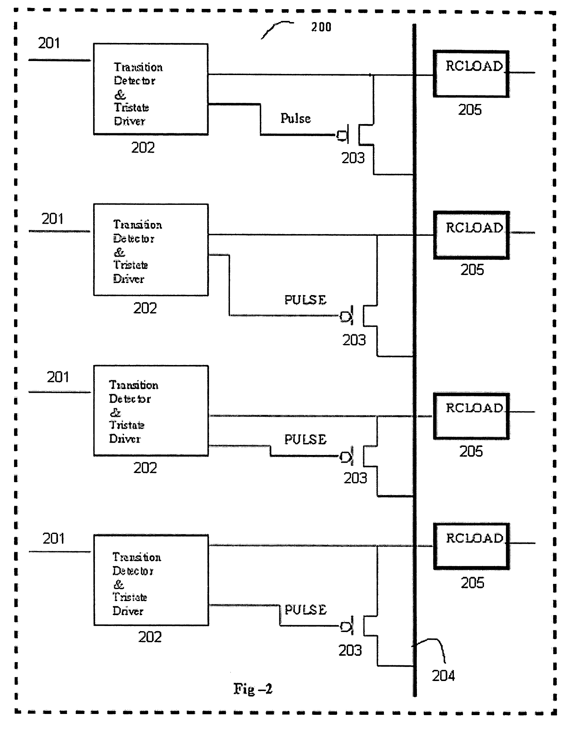
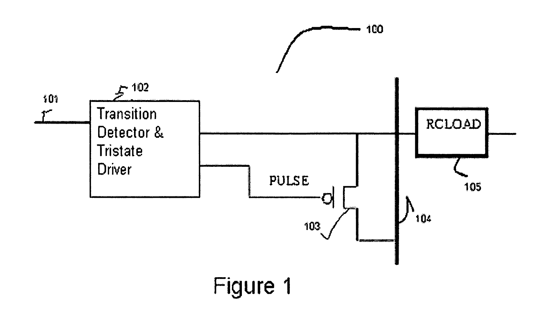
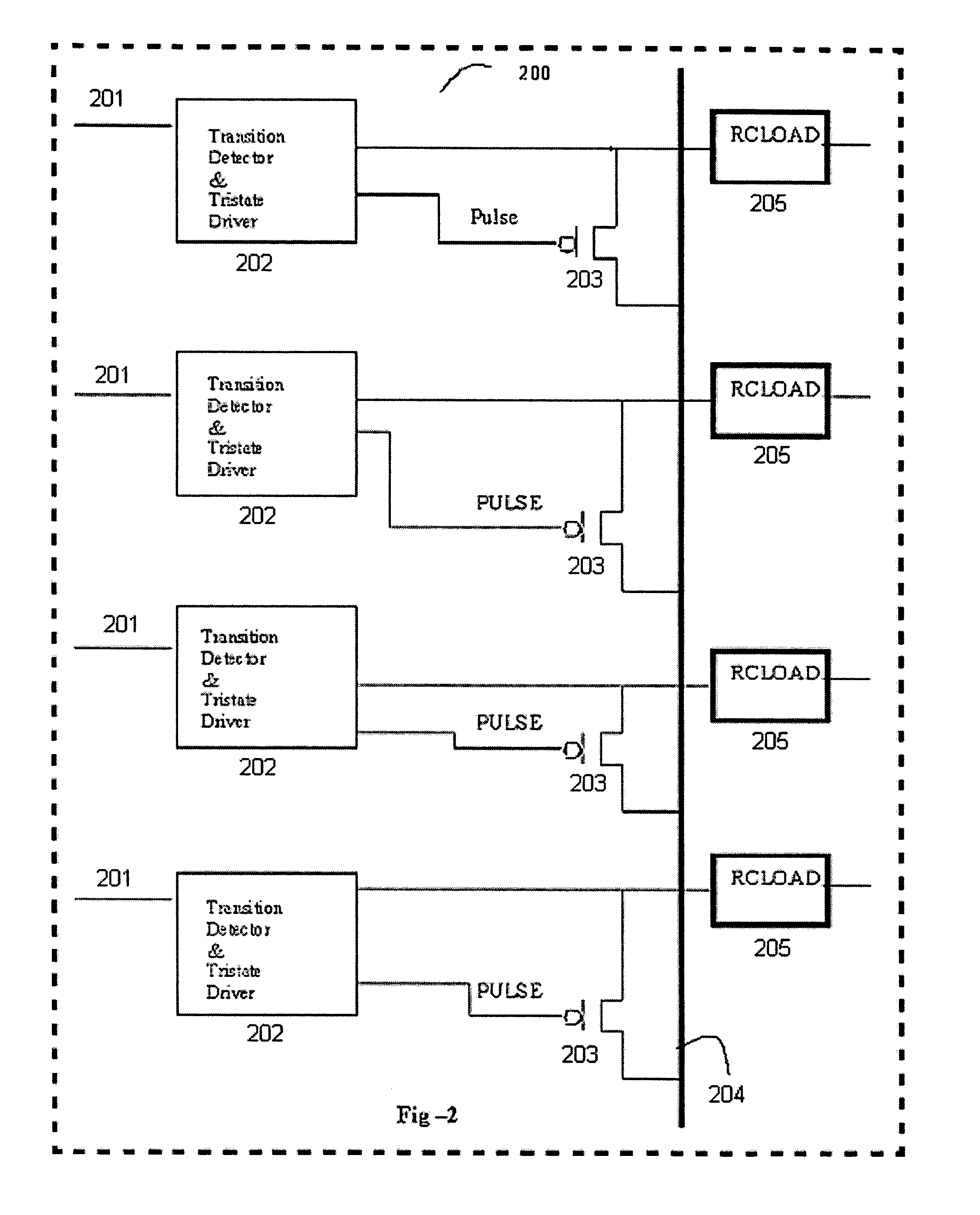
[0044]FIG. 1 shows a system for reducing power consumption in digital circuits 100 using charge redistribution for transistion of signal line 101. The said charge redistribution circuit 102 comprising transition detector and tristate driver including a control switch 103. The arrangement of transition detector, tristate driver and the switch being such that whenever the signal line 101 undergoes a transition, the charge redistribution circuit sets the source of the signal line to a high impedence and connects the signal line 101 to the floating virtual source / sink 104 for a per...


PUM


Abstract

A method and system for reducing power consumption in digital circuits using charge redistribution include a plurality of signal lines, an intermediate floating virtual source/sink, and a charge redistribution circuit connected to each signal line that isolates the signal line from its source and connects it to the intermediate floating virtual source/sink during an idle period prior to a change of state.
This charge redistribution provides steady state statistical independent advantage due to charge recycling without inserting extra complimentary lines.

Description

TECHNICAL FIELD OF THE INVENTION[0001]This invention relates generally to a method and system for reducing power consumption in digital circuitry using charge redistribution circuits.BACKGROUND OF THE INVENTION[0002]Advancements in LSI (“Large Scale Integrated”) technology continuously bring about reduced transistor sizes and corresponding many-fold increase in the number of transistors that can be mounted on a single chip. However, even though power supply voltage has been lowered considerably, the combination of size and transistor count is such that chip power consumption continues to grow resulting in increased concern with power consumption and dissipation. Power consumption and dissipation concerns have become a limiting factor in the design of LSIs used in microprocessors and other devices that require large-scale, high-speed processing. Thus, reducing power consumption has become a major priority throughout the field of LSI-related development, ranging from computer systems ...

Claims


Application Information

Patent Timeline
IPC IPC(8): H03B1/00G11C5/06H03K19/00
CPCG11C5/063H03K19/0019
Inventor NAUTIYAL, VIVEKKUMAR, ASHISH
Owner STMICROELECTRONICS PVT LTD
Why Eureka
Try Eureka