
Eureka
For R&D, Eureka makes reading and utilizing patents & technical documents easy.
Eureka AIR
Designed for self-driven R&D workflows. Generate viable solutions, solve complex R&D challenges, empower your innovation with AI.

Eureka Materials
Designed for material experts only. Revolutionize your material R&D, from search, analyze, to developing new materials.

TechResearch
Generate reliable direction feasibility study reports for your R&D in just a few steps.

TechSeek
Discover and master advanced knowledge NOW. Basics, ideas, possibilities, all at once.

TechMind
As an expert in R&D Theories, TechMind can generates customized viable solutions instantly.

TechRisk
Analyze your overall solution with one click, know your potential R&D risks in advance.

TechMonitor
Get weekly tech updates, stay abreast of the latest tech innovations and key insights.
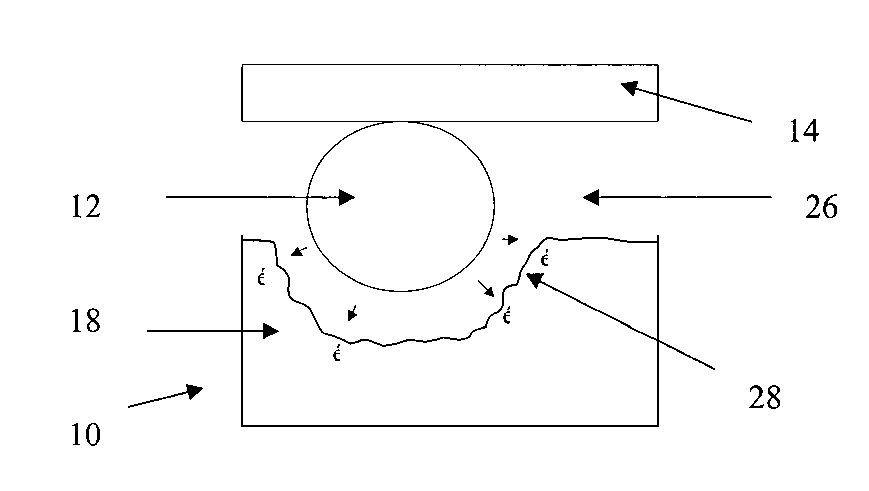
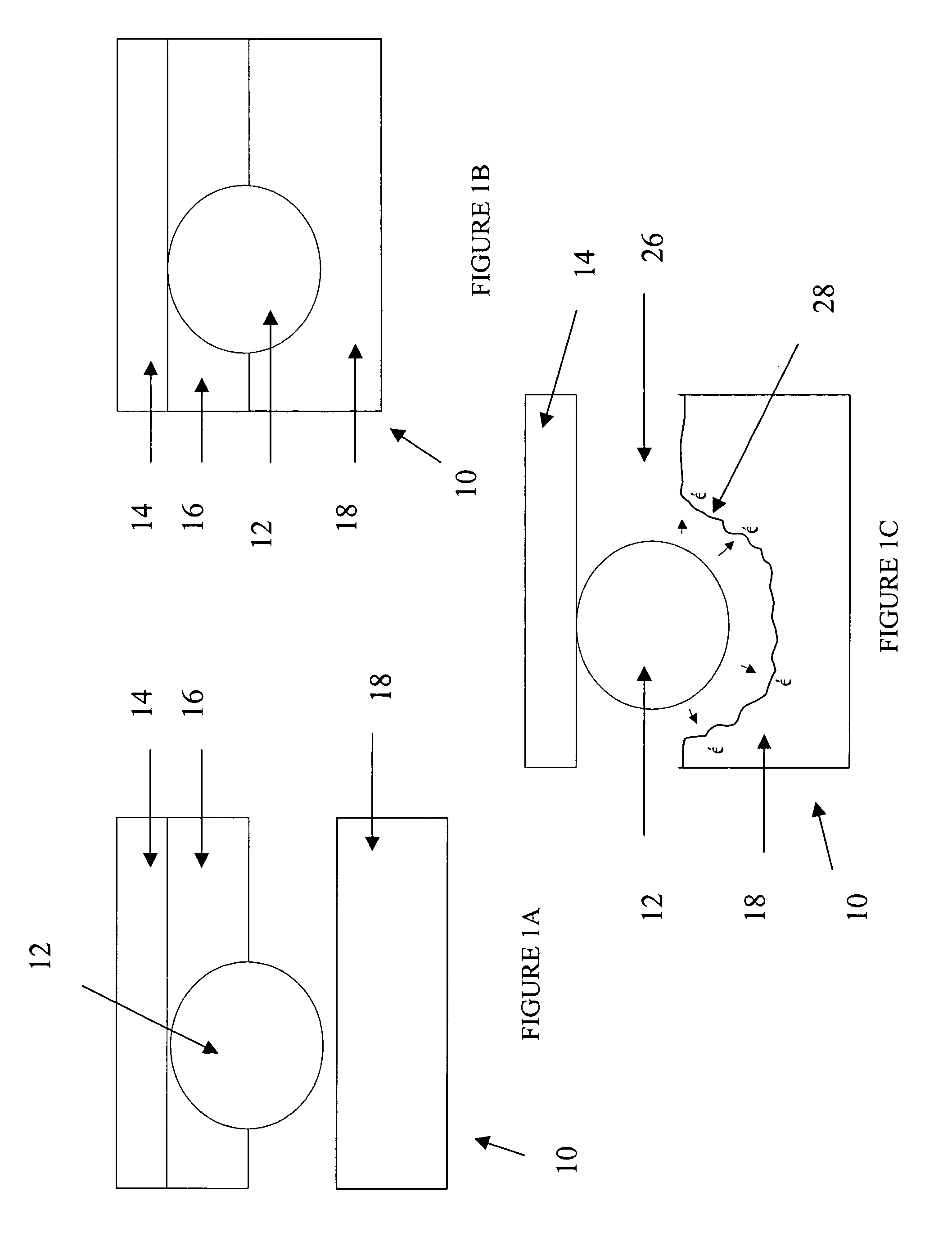
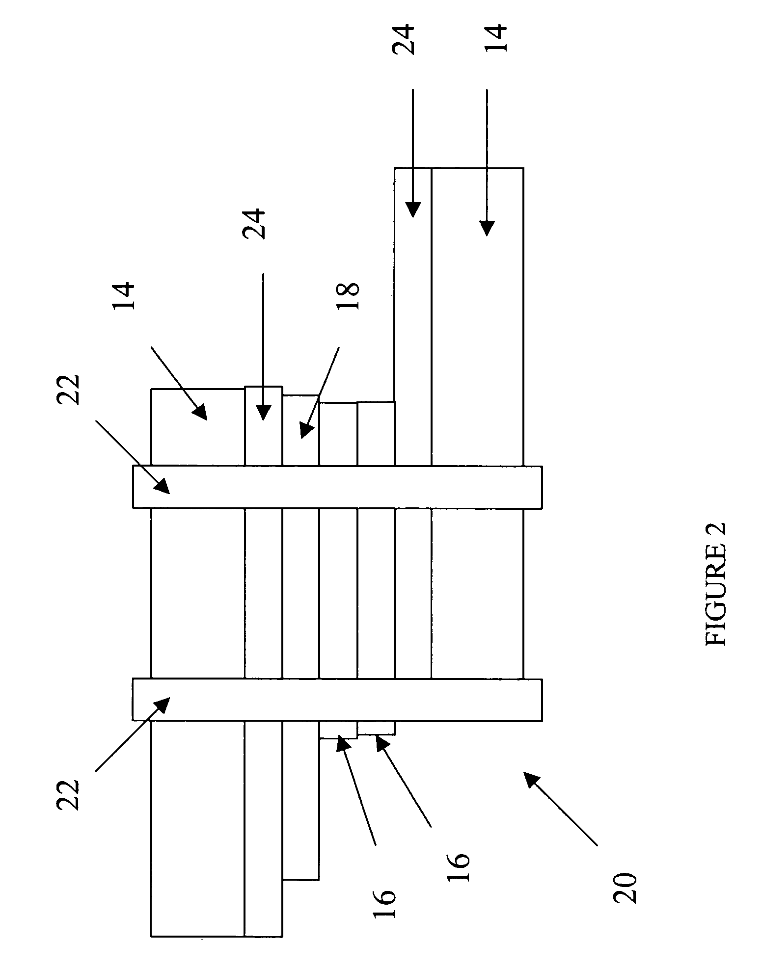
Surface imprinted films with carbon nanotubes
- Summary
- Abstract
- Description
- Claims
- Application Information
AI Technical Summary
Benefits of technology
Problems solved by technology
Method used
Image

Examples
examples
[0034]Substrates were prepared and cleaned. The preparation of the Sol-gel and conjugated polymer solutions were formulated and desired micro- and nano-structured molecules were dispersed in these solutions.
[0035]Substrates chosen for this embodiment were fluorine-doped tin oxide (SnO2:F) coated glass purchased from Hartford Glass cut to size 3 inches by 1 inch. The substrates were cleaned by immersion in dilute alconox solution (detergent) at 50° C. for 1 hour, followed by rinsing with ultrapure water (17.9 Mega Ohm resistivity), isopropanol, chloroform, and absolute ethanol (absolute being 200 proof).
[0036]The sol-gel solution was prepared by mixing 9.8 mL ethanol (100%), 250 μL ultrapure H2O, and 1 drop of concentrated nitric acid (HNO3) in a vial. It was desirable to include an alcohol and water mix ratio of about (1:0.025). Nitric acid was utilized for acidification of the alcohol / water mix. The vial was then transferred to a glove-box purged with N2 gas for approximately 1 to ...
PUM
| Property | Measurement | Unit |
|---|---|---|
| Thickness | aaaaa | aaaaa |
| Thickness | aaaaa | aaaaa |
| Thickness | aaaaa | aaaaa |
Abstract
Description
Claims
Application Information
 - R&D Engineer
- R&D Manager
- IP Professional
- Industry Leading Data Capabilities
- Powerful AI technology
- Patent DNA Extraction
Browse by: Latest US Patents, China's latest patents, Technical Efficacy Thesaurus, Application Domain, Technology Topic, Popular Technical Reports.
© 2024 PatSnap. All rights reserved.Legal|Privacy policy|Modern Slavery Act Transparency Statement|Sitemap|About US| Contact US: help@patsnap.com