Methods, systems and structures for forming improved transistors

a technology of transistors and transistors, applied in the field of semiconductor devices, can solve the problems of increasing scattering, reducing the mobility advantages of strained channels, and unable to achieve the relaxation layer, so as to improve the operation of devices

Active Publication Date: 2006-10-17
TEXAS INSTR INC
View PDF18 Cites 46 Cited by
  • Summary
  • Abstract
  • Description
  • Claims
  • Application Information

AI Technical Summary

Benefits of technology

[0008]New and improved methods and systems are provided for forming strain in selected semiconductor device regions to improve the operation of the devices.

Problems solved by technology

The ability to form a relaxed SiGe layer is important in obtaining an overlying, epitaxially grown, silicon layer under biaxial tensile strain, however the attainment of the relaxed SiGe layer can be costly and difficult to achieve.
A disadvantage of this method is that carbon within the channel portion of the strain layer can migrate into the overlying gate oxide, thereby causing a relatively large interface trap density (DIT), which disadvantageously increases scattering and reduces the mobility advantages associated with the strained channel.
Another important issue with this approach is the problem of getting the C atoms in substitutional lattice site in silicon.

Method used


Image

  • Methods, systems and structures for forming improved transistors
  • Methods, systems and structures for forming improved transistors
  • Methods, systems and structures for forming improved transistors

Examples


Embodiment Construction

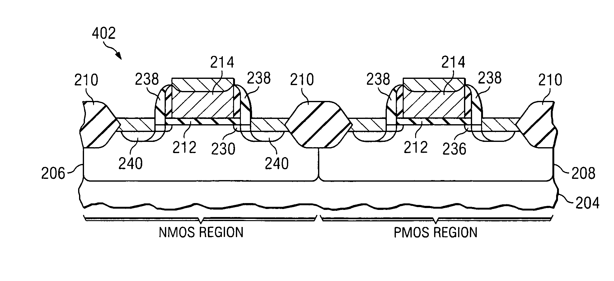
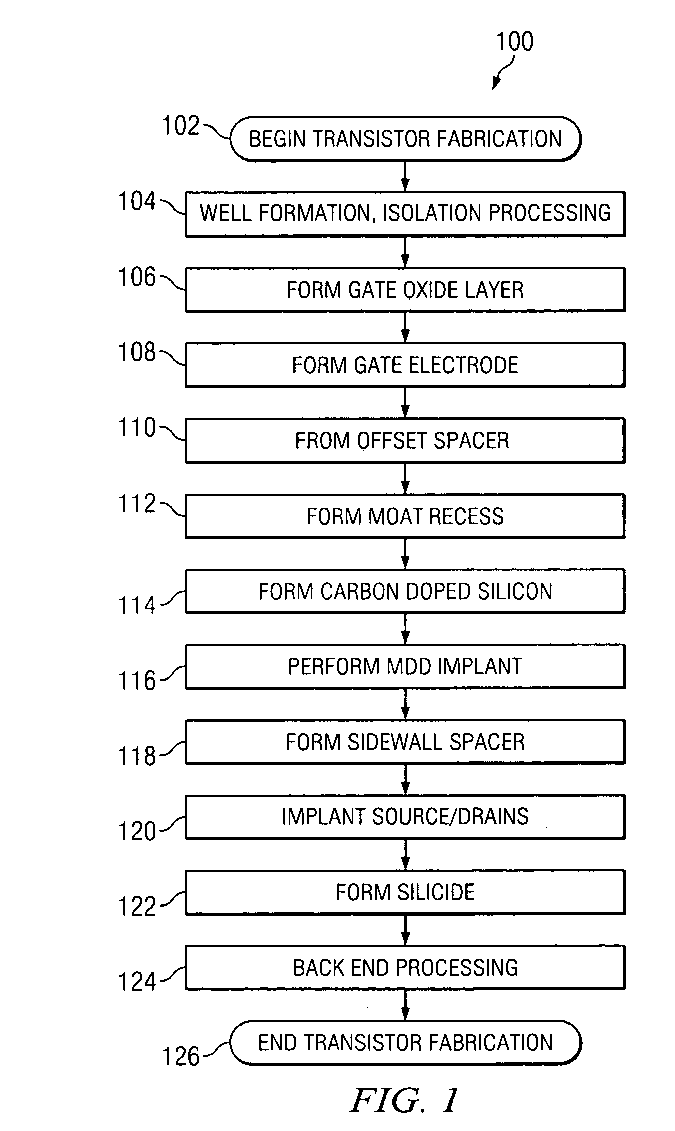
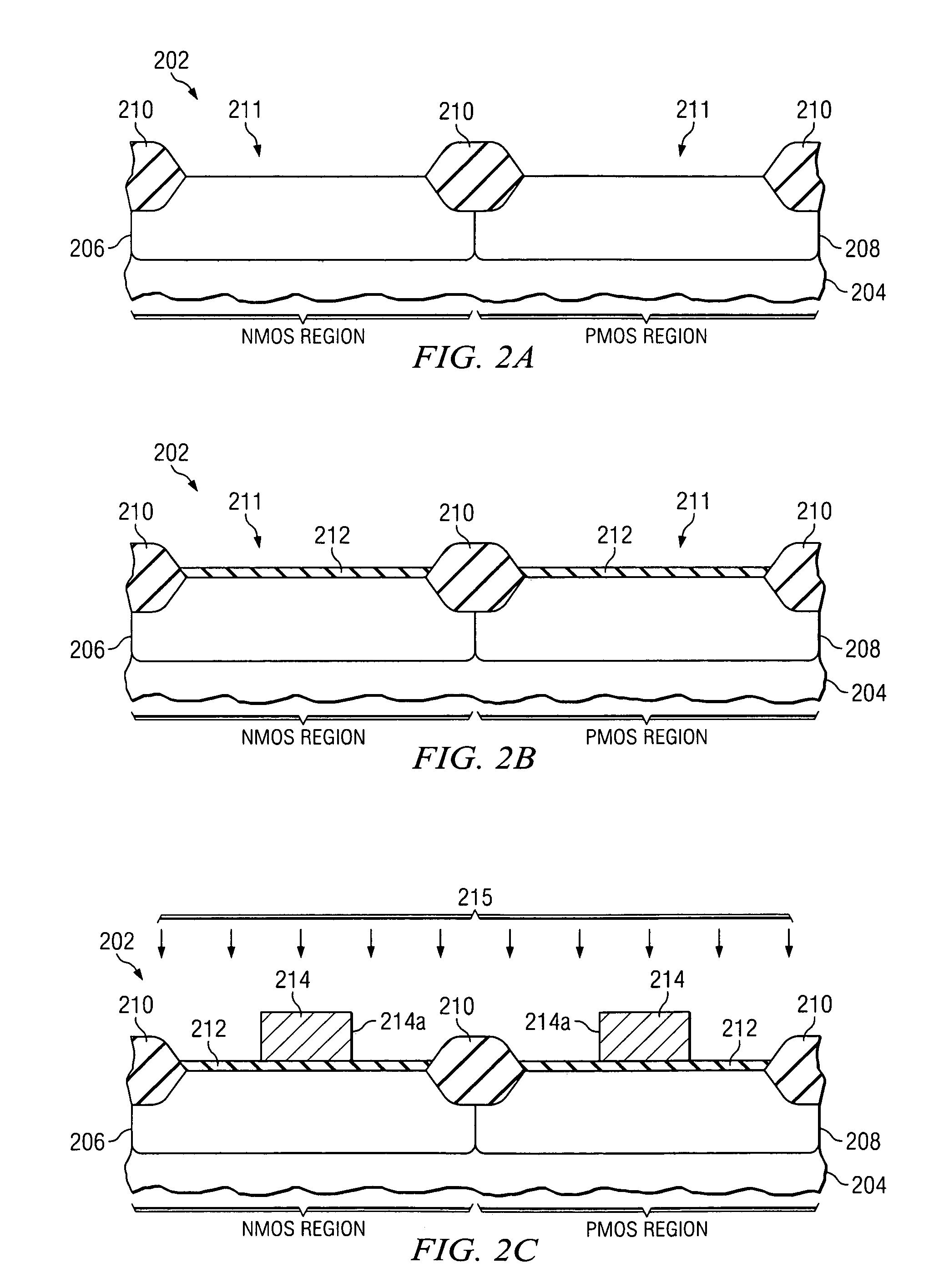
[0018]One or more implementations of the present invention will now be described with reference to the attached drawings, wherein like reference numerals are used to refer to like elements throughout, and wherein the illustrated structures are not necessarily drawn to scale. The invention provides transistor structures and methods exhibiting improved operating characteristics in which it is theorized that transistor mobility is improved while minimizing defects heretofore associated with conventional strained silicon device solutions.

[0019]The present inventors have determined that the operation of an FET is improved through manufacture and structure in accordance with the invention described below. While the inventors theorize that the beneficial results of the invention are obtained through the substitution of dopant atoms at an atomic level for silicon atoms within the semiconductor crystal lattice structure, resulting in the inducement of strain and concomitantly enhanced carrie...


PUM


Abstract

A method (100) of forming a transistor includes forming a gate structure (106, 108) over a semiconductor body and forming recesses (112) substantially aligned to the gate structure in the semiconductor body. Amorphous silicon regions are then formed (114) in the recesses. The amorphous silicon regions are re-crystallized. Sidewall spacers are formed (118) over lateral edges of the gate structure. The method continues by implanting source and drain regions in the semiconductor body (120) after forming the sidewall spacers. The re-crystallized silicon regions formed in the recesses reside close to the transistor channel and serve to facilitate improved carrier mobility in NMOS type transistor devices.

Description

FIELD OF INVENTION[0001]The present invention relates generally to semiconductor devices and more particularly to FET transistors and associated methods of manufacture having improved drain / source structures.BACKGROUND OF THE INVENTION[0002]A conventional field effect transistor (FET), also known as a metal oxide semiconductor (MOS) transistor, generally includes a semiconductor substrate, such as silicon, having a source, a drain, and a channel positioned between the source and drain. A gate stack composed of a conductive material (a gate conductor), an oxide layer (a gate oxide), and sidewall spacers, is typically located above the channel. The gate oxide is typically located directly above the channel, while the gate conductor, generally comprised of polycrystalline silicon (polysilicon) material, is located above the gate oxide. The sidewall spacers protect the sidewalls of the gate conductor.[0003]Generally, for a given electric field across the channel of a MOS transistor, the...

Claims


Application Information

Patent Timeline
Patent Type & Authority Patents(United States)
IPC IPC(8): H01L21/336
CPCH01L21/823807H01L21/823814H01L29/6659H01L29/66636H01L29/7833H01L29/7842H01L29/7848
Inventor CHIDAMBARAM, PRBU, HAOWEN
Owner TEXAS INSTR INC
Why Eureka
Try Eureka