Memory device capable of performing high speed reading while realizing redundancy replacement
a memory device and redundancy replacement technology, applied in semiconductor devices, digital storage, instruments, etc., can solve the problems of high speed access, deterioration of access performance, and degradation of possible speed, so as to minimize fluctuations in the electric resistance of read current paths, improve the read margin and access time, and minimize imbalances in parasitic capacitance.
- Summary
- Abstract
- Description
- Claims
- Application Information
AI Technical Summary
Benefits of technology
Problems solved by technology
Method used
Image
Examples
first embodiment
[0092
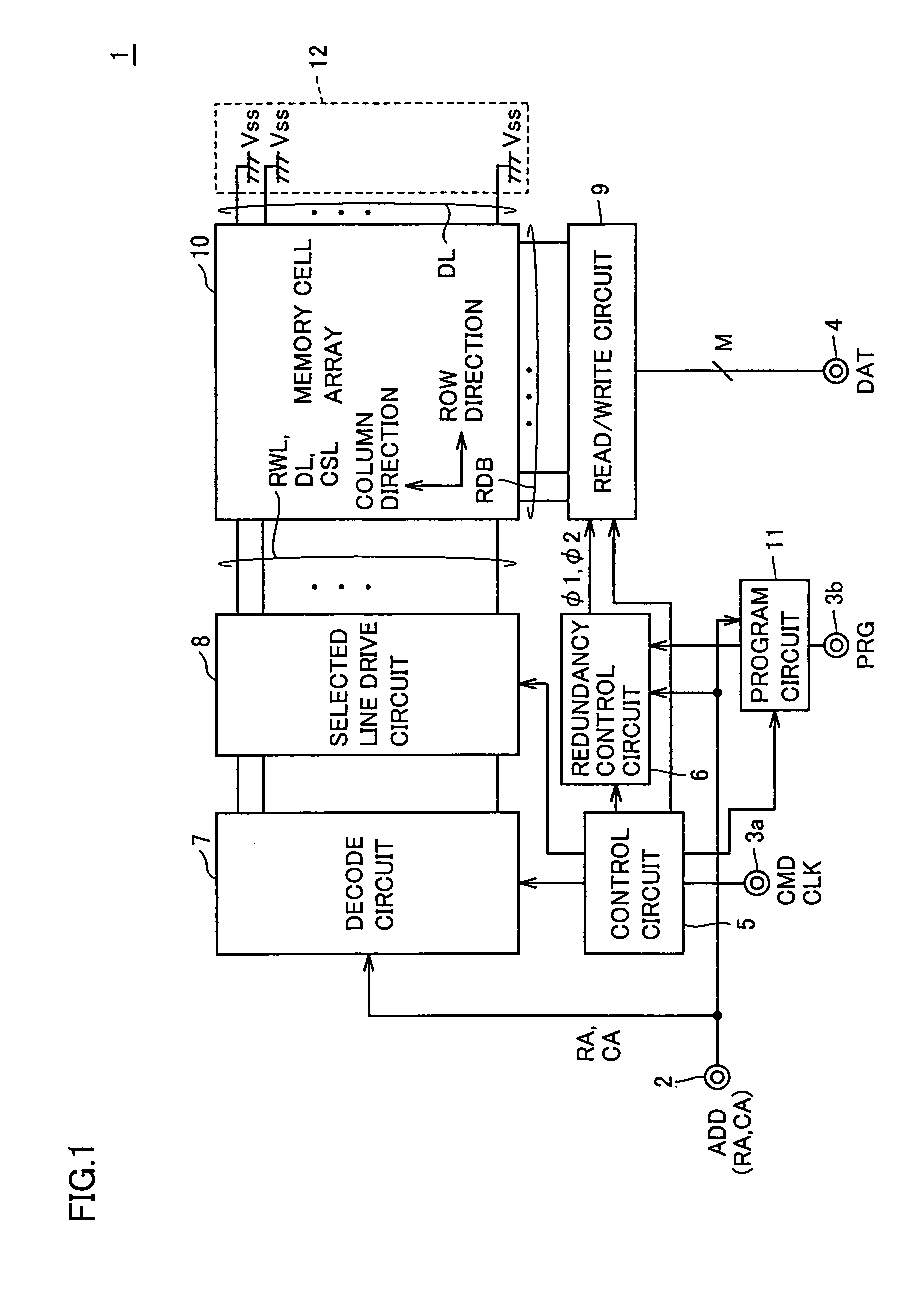
[0093]FIG. 1 is a schematic block diagram showing an overall architecture of an MRAM device 1 of a first embodiment of the present invention.
[0094]Referring to FIG. 1, MRAM device 1 performs supply / reception of a data signal DAT of M bits (wherein M is a natural number) according to a control signal CMD and an address signal ADD from outside. A data read operation and a data write operation in MRAM device 1 are performed at timings in synchronization with, for example, a clock signal CLK from outside. Alternatively, operation timings may be internally determined without receiving clock signal CLK from outside.
[0095]MRAM device 1 includes: an address terminal 2 receiving an input of address signal ADD; a signal terminal 3a receiving inputs of control signal CAD and clock signal CLK; a signal terminal 3b receiving an input of a program signal PRG activated in a program operation; and a data terminal 4 performing supply / reception of data signal DAT of M bits.
[0096]MRAM device 1 fu...
second embodiment
[0187
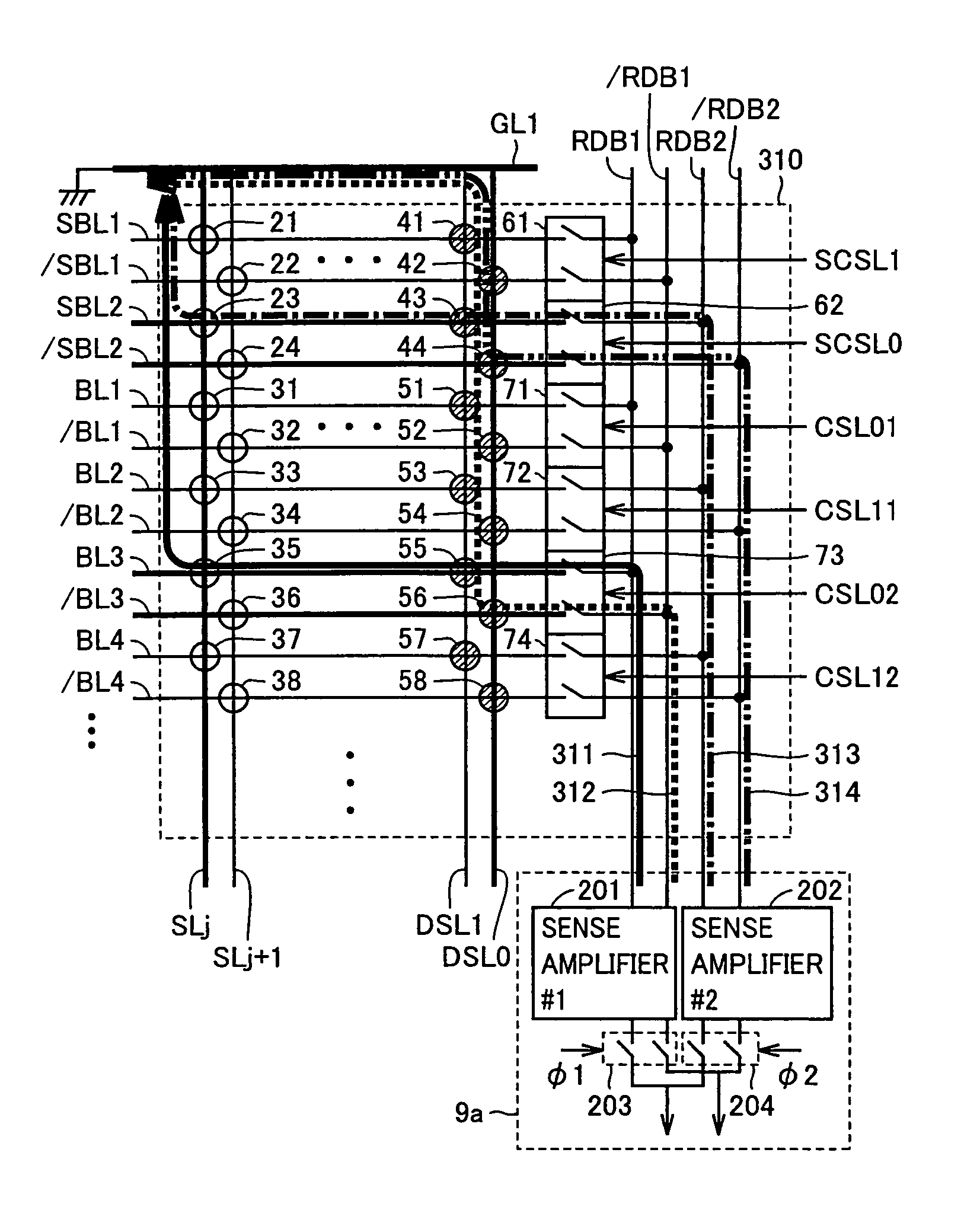
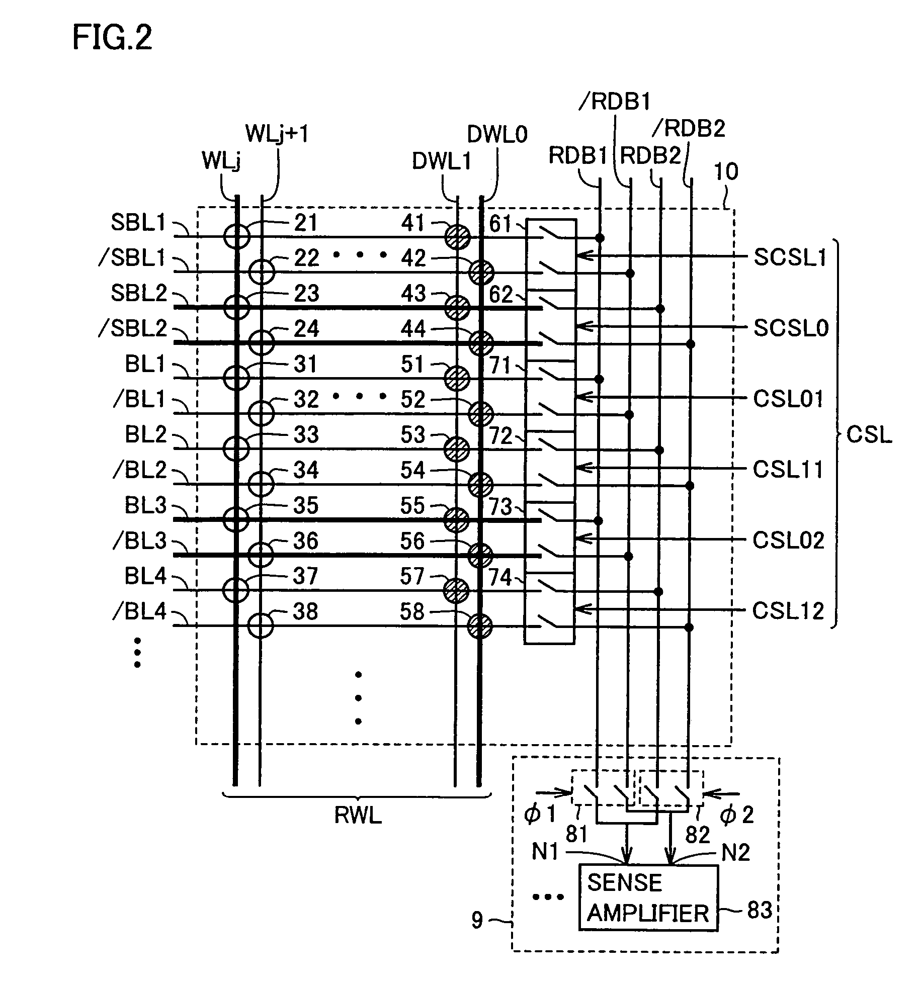
[0188]Description has been given of a case where simultaneous parallel access operations on a normal memory cell and a spare memory cell in the first embodiment. In this case, an imbalance occurs in read speed between memory cells if lengths of current paths along which read currents flow are different from each other according to locations of memory cells on which parallel accesses are made. If an imbalance in read speed occurs, an access time is limited by a memory cell with the slowest read speed; therefore, an access time is eventually deteriorated.
[0189]FIG. 16 is a circuit diagram showing a configuration of a memory cell array 310 used in a second embodiment. Note that the configuration shown in FIG. 16 is provided with a plurality of stages of sense amplifiers corresponding to the respective read data bus pairs as shown in FIG. 9 and effective in a case where read currents flow simultaneously through a plurality of read data buses.
[0190]While in FIG. 9, word lines and du...
third embodiment
[0210
[0211]In the first embodiment, description has been given of a case where simultaneous accesses are made to a normal memory cell and a spare memory cell. At this time, there arises a problem that an accesses time is deteriorated by electric resistance of a superimposed portion, especially a common source line, of a plurality of read current paths accessed in parallel.
[0212]That is, when 2 currents flowing in a normal memory cell and a spare memory cell flow through the same source line, a float of a source potential is doubled to thereby delay a access time to be longer. In this case, it is only required to arrange source lines and word lines so as to separate a path of a current flowing in a normal memory cell and a path of a current flowing in a spare memory cell from each other at all times.
[0213]FIG. 22 is a circuit diagram showing a configuration of a memory cell array 610 used in a third embodiment in which a read current path is separated.
[0214]Referring to FIG. 22, memo...
PUM
 Abstract
Description
Claims
Application Information
 - R&D
- Intellectual Property
- Life Sciences
- Materials
- Tech Scout
- Unparalleled Data Quality
- Higher Quality Content
- 60% Fewer Hallucinations
Browse by: Latest US Patents, China's latest patents, Technical Efficacy Thesaurus, Application Domain, Technology Topic, Popular Technical Reports.
© 2025 PatSnap. All rights reserved.Legal|Privacy policy|Modern Slavery Act Transparency Statement|Sitemap|About US| Contact US: help@patsnap.com


