Photodetectors, optical modules, and optical transmission devices

a technology of optical modules and optical transmission devices, applied in the direction of optical radiation measurement, instruments, spectrophotometry/monochromators, etc., can solve the problems of difficult to obtain a high photodetecting sensitivity and thin thickness of each layer, so as to reduce the delay in group velocity of photoabsorption wavelengths, and reduce the refractive index of the photoabsorption layer composed of semiconductors

Inactive Publication Date: 2006-10-31
SEIKO EPSON CORP
View PDF3 Cites 7 Cited by
  • Summary
  • Abstract
  • Description
  • Claims
  • Application Information

AI Technical Summary

Benefits of technology

[0009]According to an exemplary aspect of the present invention, the multilayer film has a one-dimensional photonic crystal structure due a cyclic structure of the high refractive index layers and the low refractive index layers. A photonic band gap, that prohibits the propagation of light in a certain wavelength region, is created in the direction in which the layers are stacked. In the photonic crystal structure, the density state of photons rise and the group velocity is delayed in a band edge of a photonic band. Specifically, in accordance with an exemplary aspect of the present invention, the multilayer film is introduced as an optical delaying film, which is provided with a function to absorb light, whereby the time that light stays in the photoabsorption layer is extended to several times longer than usual or greater, such that the sensitivity can be enhanced. Also, in accordance with an exemplary aspect of the present invention, the photodetector has a MSM structure, such that the advancing direction of light and the traveling direction of electrons are arranged in different directions. Accordingly, electrons travel in the semiconductor layer, which has a relatively low-resistance. Therefore a high-speed responsiveness can be sufficiently maintained.
[0017]In the photodetector in accordance with an exemplary aspect of the present invention, the electrodes may have a planar configuration in a comb shape. As a result, the distance between the electrodes can be shortened, and their opposing area can be increased, such that a high-speed responsiveness can be obtained, and the light receiving efficiency can be enhanced.

Problems solved by technology

However, because the MSM type photodiode has a structure in which its light receiving surface is covered with the electrode, it is difficult to obtain a high photodetecting sensitivity.
However, when the super-lattice structure is used, the thickness of each of the layers becomes very thin by the mismatch in the lattice constants of the materials.

Method used


Image

  • Photodetectors, optical modules, and optical transmission devices
  • Photodetectors, optical modules, and optical transmission devices
  • Photodetectors, optical modules, and optical transmission devices

Examples


exemplary embodiment 1

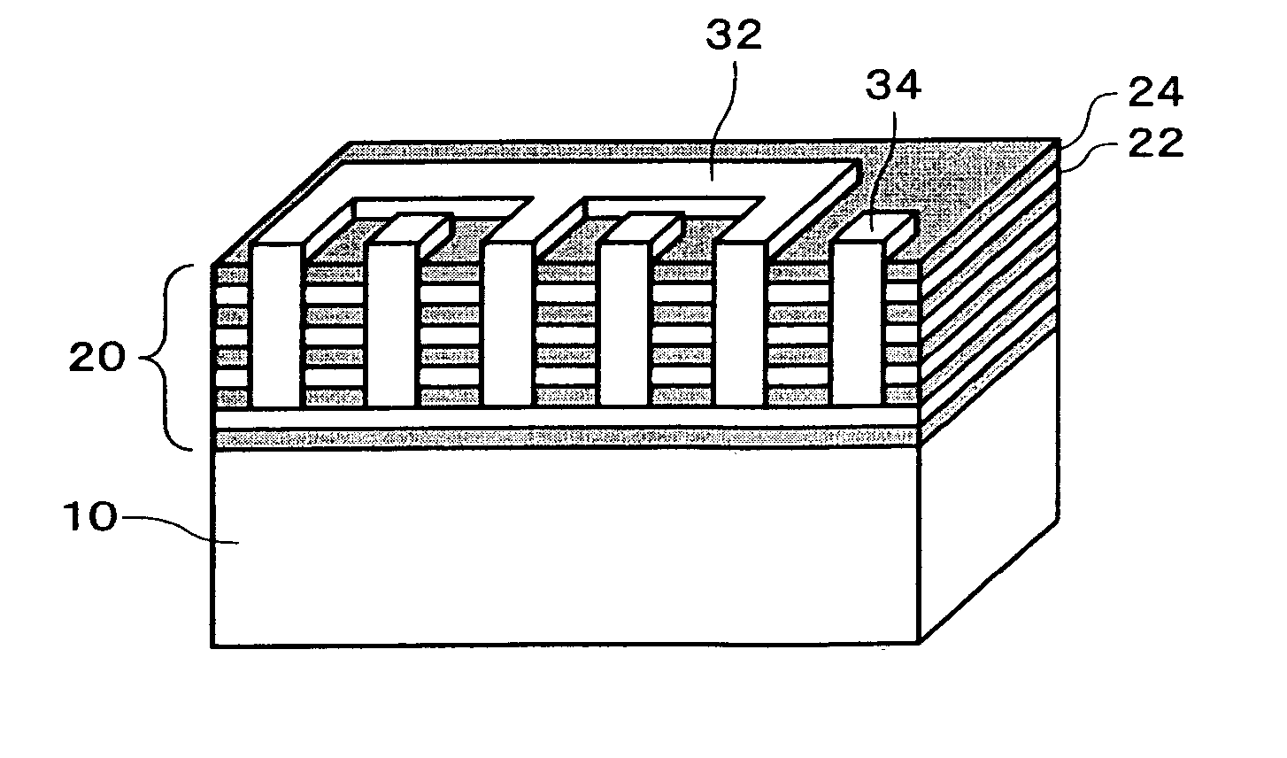
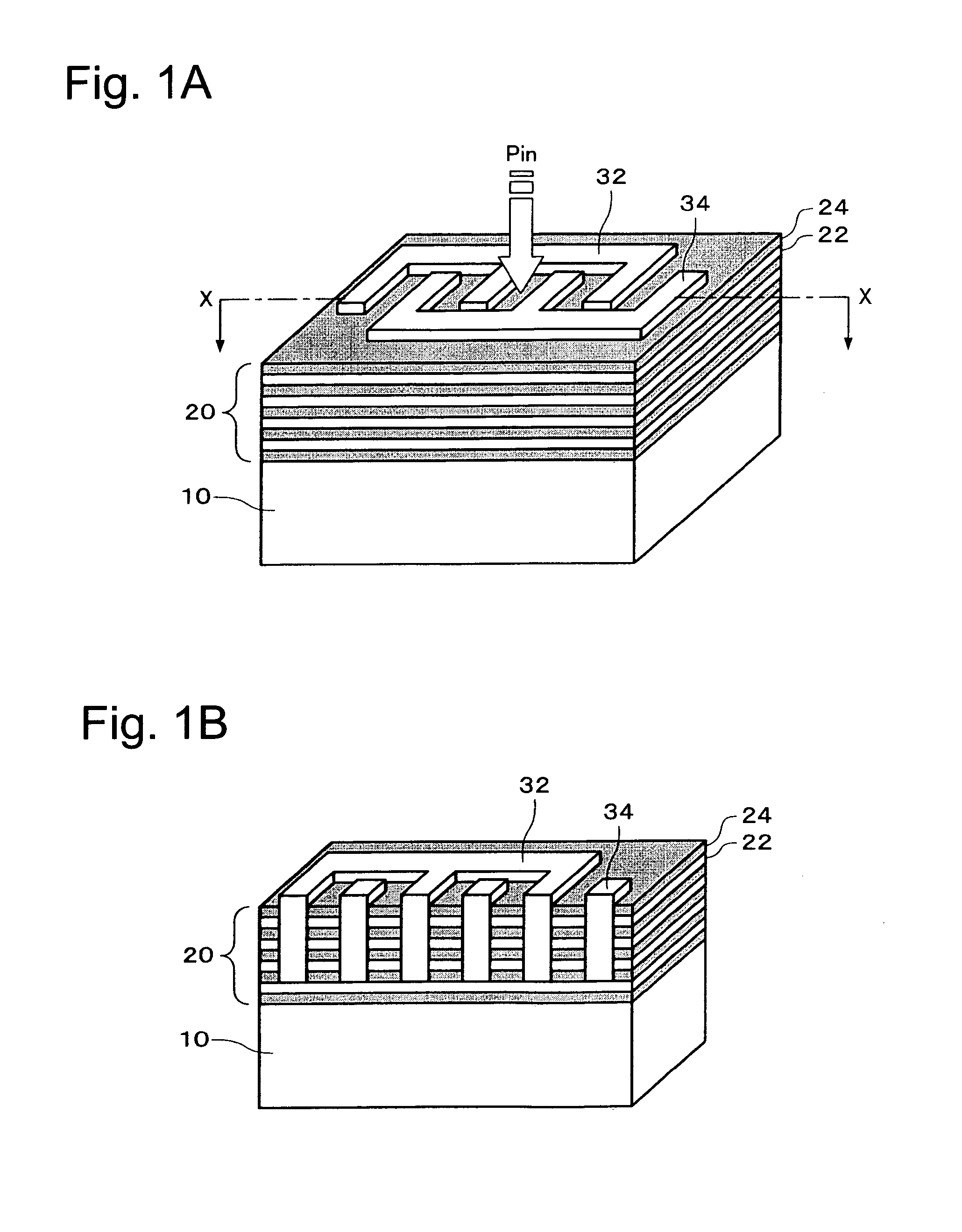
[0050]As an exemplary embodiment of the photodetector of the present invention, a case in which a multilayer film formed from GaAs / AlxOy is used is described below.

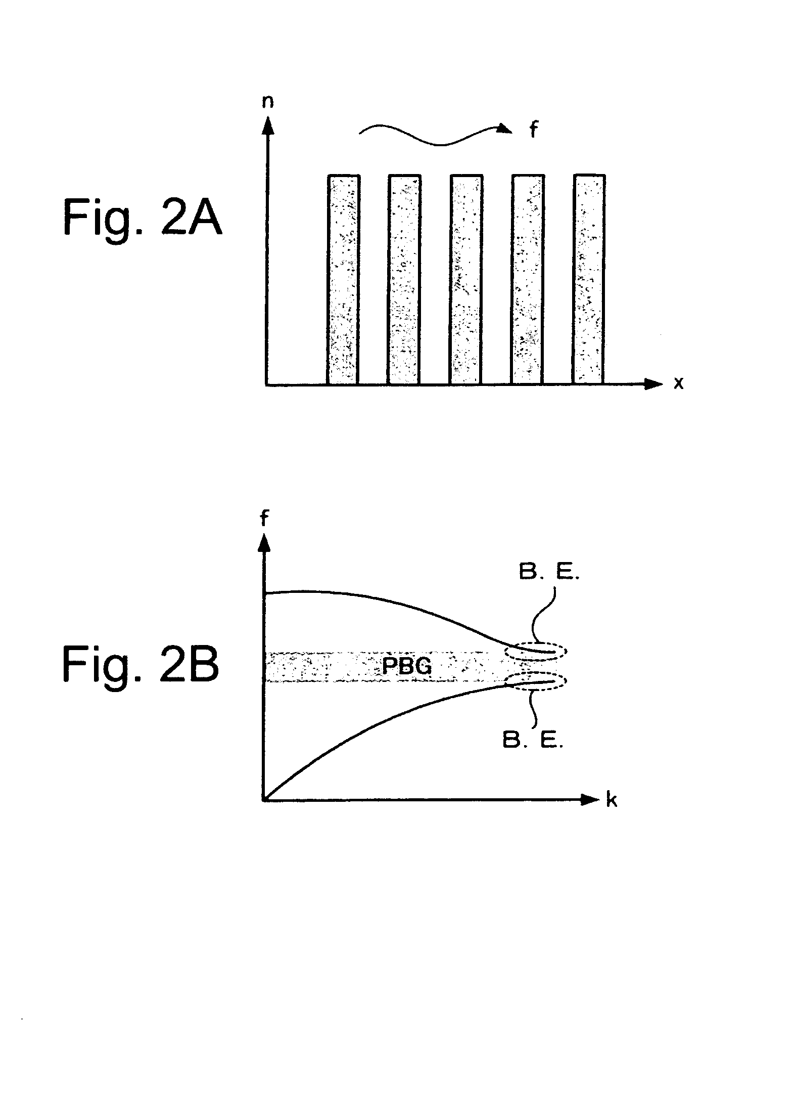
[0051]First, manufacturing of the device is described. This is conducted according the procedure indicated in FIG. 6A–FIG. 6D. First, a GaAs / AlAs multilayer film is grown on a GaAs substrate. The unit cycle length of the multilayer film is set such that the absorption band of the GaAs layer that becomes a photoabsorption layer in the low group velocity wavelength region is included in the photonic band structure of the GaAs / AlxOy multilayer film shown in FIG. 7. In FIG. 7, a is the thickness of one pair (unit cycle of the photonic crystal), and c is a velocity of light. The multilayer film may be formed in a manner that the thickness of each of the films is gradually changed in the wavelength region that causes the reduced group velocity, so that the group velocity may gradually become smaller. In any case, the length of ...


PUM

PropertyMeasurementUnit
wavelengthaaaaaaaaaa
lengthaaaaaaaaaa
absorption coefficientaaaaaaaaaa

Abstract

A method is provided to provide a photodetector that can enhance the light receiving sensitivity with a relatively simple structure, and that can maintain a high speed responsiveness. A photodetector having a MSM (Metal-Semiconductor-Metal) structure, including a substrate, a multilayer film that is disposed over the substrate and includes a low refractive index layer and a high refractive index layer that are alternately laminated as a unit cycle. At least one of the low refractive index layer and the high refractive index layer is a photoabsorption layer composed of semiconductor, and a portion that is embedded in the multilayer film, the portion having at least one pair of opposing electrodes within the multilayer film. The multilayer film is formed such that a wavelength region corresponding to a band edge of a photonic band overlaps at least a part of an absorption band of the photoabsorption layer, to thereby delay a group velocity of incidence light Pin with a predetermined wavelength that belongs to the absorption band of the photoabsorption layer.

Description

RELATED APPLICATIONS[0001]The present application claims priority to Japanese Patent Application No. 2003-383733 filed Nov. 13, 2003 which is incorporated by reference in its entirety.BACKGROUND OF THE INVENTION[0002]1. Field of Invention[0003]Exemplary aspects of the present invention relate to photodetectors, optical modules and optical transmission devices having a MSM (Metal-Semiconductor-Metal) structure.[0004]2. Description of Related Art[0005]A related art MSM type photodiode uses a comb-shaped electrode to apply a high electric field with a low voltage to a photoabsorption layer, and realizes a high-speed responsiveness with its short traveling distance of electrons. For this reason, the MSM type photodiodes are promising as photodetectors in optical transmission devices, optical interconnection, etc.SUMMARY OF THE INVENTION[0006]However, because the MSM type photodiode has a structure in which its light receiving surface is covered with the electrode, it is difficult to obt...

Claims


Application Information

Patent Timeline
Patent Type & Authority Patents(United States)
IPC IPC(8): G02F1/03G02F1/07G06F1/03H01L31/00H01L31/0216H01L31/108
CPCH01L31/02162H01L31/1085
Inventor MOCHIZUKI, MASAMITSUKOYAMA, TOMOKOONISHI, HAJIME
Owner SEIKO EPSON CORP
Why Eureka
Try Eureka