Charge modulation network for multiple power domains for silicon-on-insulator technology

a technology of silicon-on-insulator and charge modulation network, which is applied in the direction of semiconductor devices, semiconductor/solid-state device details, electrical apparatus, etc., can solve the problems of degradation of yield and reliability of integrated circuits, damage to gate dielectrics, and charge damage in soi devices, so as to achieve the effect of mitigating the accumulation of electrical charges

Inactive Publication Date: 2006-10-31
GLOBALFOUNDRIES INC
View PDF21 Cites 42 Cited by
  • Summary
  • Abstract
  • Description
  • Claims
  • Application Information

AI Technical Summary

Benefits of technology

[0016]Broadly, in accordance with one aspect of the invention, there is disclosed a method of implementing electrostatic discharge protection in a silicon-on-insulator (SOI) integrated circuit comprising: providing a first power domain and a second power domain in the SOI integrated circuit; and providing a charge modulation network in the SOI integrated circuit between the first power domain and the second power domain to mitigate accumulation of electrical charge in an electrically isolated region of the SOI integrated circuit.
[0021]There is disclosed in accordance with another aspect of the invention an SOI integrated circuit including ESD protection comprising an SOI chip. A first power domain and a second power domain are provided in the SOI chip. A charge modulation network in the SOI chip between the first power domain and the second power domain mitigates accumulation of electrical charge in an electrically isolated region of the SOI chip.

Problems solved by technology

Charge damage from plasma processes can degrade yield and reliability of integrated circuits.
For devices fabricated on bulk Si, a charge differential can develop between the gate electrode and the substrate, resulting in large current flow through the gate dielectric, and hence damage to the gate dielectric.
However, charge damage can occur in SOI devices if the gate charges to a different potential than the diffusions.
This differential charging can result in damage to the gate dielectric, and reduces yield.
At present, there is no method to protect devices on SOI from differential charging when gates and diffusions are connected to different power or ground grids.
Charge buildup from plasma etching can lead to destruction of semiconductor components.
Charging issues which are normally not a concern in bulk CMOS can become an issue in SOI technology.
A key issue is the problem of a power grid which is isolated or disconnected.
Despite the advantages obtained using SOI technology, SOI circuits, like other electronic devices, are susceptible to electrostatic discharge (ESD), i.e. a surge in voltage (negative or positive) that occurs when a large amount of current is applied in the circuit.
Moreover, the handling of SOI devices themselves may lead to charging of the substrate.
Traditional bulk overvoltage protection schemes, such as diodes, do not work well on SOI because of the presence of the relatively thin diffusion over the buried oxide layer.
That is, conventional diodes on SOI devices have small current drivability because the current is carried laterally (limited by the thickness of the semiconductor material).
Although the diode disclosed in Lu can provide some ESD protection, the disclosed diode does not allow for obtaining ideal diode characteristics.
In cases wherein the heat becomes too excessive, destruction of the SOI circuit may occur.

Method used


Image

  • Charge modulation network for multiple power domains for silicon-on-insulator technology
  • Charge modulation network for multiple power domains for silicon-on-insulator technology
  • Charge modulation network for multiple power domains for silicon-on-insulator technology

Examples


Embodiment Construction

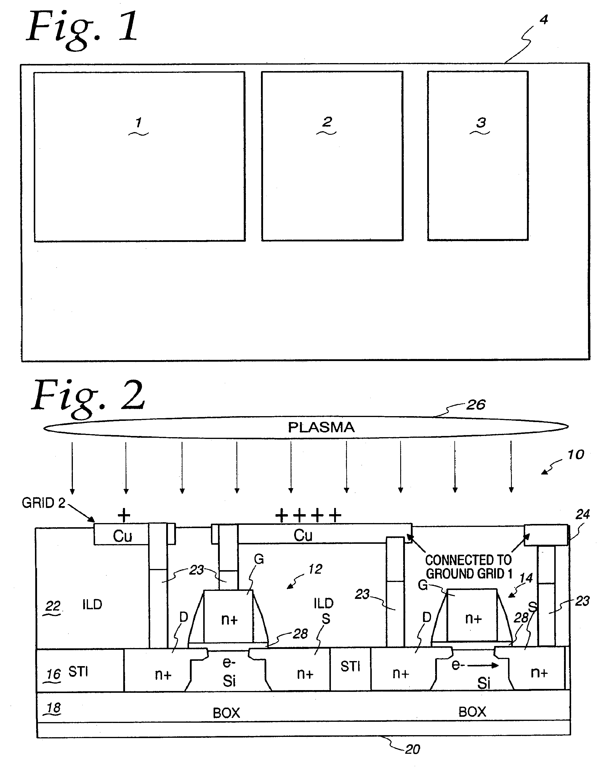
[0045]Referring initially to FIG. 1, a plurality of blocks 1, 2 and 3 are illustrated as a sub part of a larger block 4. The larger block 4 may comprise, for example, a wafer with blocks 1, 2 and 3 comprising individual chips on the wafer. Alternatively, the block 4 may comprise a chip with the blocks 1, 2 and 3 representing circuit domains or regions on the chip. The blocks 1, 2 and 3 particularly represent the separation of grounds and power domains in manufacture of a silicon-on-insulator (SOI) chip. For example, the blocks 1, 2 and 3 may comprise areas, in the form of logic and / or memory, on the chip 4 supplied through separate, dedicated power feeds, also known as voltage islands. Alternatively, they may comprise areas within an island fed by the same voltage source but independently controlled via an inter-island header switch, referred to as a power domain. The teachings of the present invention are applicable to plural power domains and / or voltage islands, and for simplicity...


PUM


Abstract

An SOI integrated circuit includes ESD protection on an SOI chip. A first power domain and a second power domain are provided in the SOI chip. In one embodiment, a charge modulation network in the SOI chip between the first power domain and the second power domain mitigates accumulation of electrical charge in an electrically isolated region of the SOI chip. In another embodiment, an ESD protection device in the SOI chip electrically connects the first power domain and the second power domain via a low metal layer to provide a discharge path for accumulated charge.

Description

FIELD OF THE INVENTION[0001]The present invention generally relates to integrated circuits, and more particularly to minimize charging effects in such integrated circuits.BACKGROUND OF THE INVENTION[0002]Charge damage from plasma processes can degrade yield and reliability of integrated circuits. For devices fabricated on bulk Si, a charge differential can develop between the gate electrode and the substrate, resulting in large current flow through the gate dielectric, and hence damage to the gate dielectric. As a result, gates in bulk Si devices are often connected to protect diodes, that equalize charge between the gate and substrate during plasma processing, thereby protecting the gate dielectric from plasma damage.[0003]For devices fabricated on silicon-on-insulator (SOI) substrates, the device Si is generally isolated from the substrate. However, charge damage can occur in SOI devices if the gate charges to a different potential than the diffusions. Such differential charging c...

Claims


Application Information

Patent Timeline
Patent Type & Authority Patents(United States)
IPC IPC(8): H02H9/00
CPCH01L27/0251
Inventor CAIN, DAVID A.GAMBINO, JEFFREY P.ROHRER, NORMAN J.SEITZER, DARYL M.VOLDMAN, STEVEN H.
Owner GLOBALFOUNDRIES INC
Why Eureka
Try Eureka