Logic verification device, logic verification method and logic verification computer program

a logic verification and logic verification technology, applied in the direction of program control, cad circuit design, instruments, etc., can solve the problems of inevitably applying correction techniques that may not be the best ones, previously applied correction techniques may have to be altered, etc., to reduce the number of design steps.

Inactive Publication Date: 2006-10-31
FUJITSU LTD
View PDF7 Cites 53 Cited by
  • Summary
  • Abstract
  • Description
  • Claims
  • Application Information

AI Technical Summary

Benefits of technology

[0016]In view of the above identified problems, it is therefore an object of the present invention to provide a logic verification device, a logic verification method and a logic verification computer program that can reduce the number of steps involved in designing a logic circuit particularly when the designed logic circuit is subjected to logic verification and modification at the spot where an error is detected.
[0018]With this arrangement, it is possible to reduce the number of times of data conversions by making it possible to modify the data for verification to be processed for logic verification. Additionally, since the data for verification that have been modified can also be subjected to logic verification, it is possible to repeat an operation of logic verification and an operation of modification on the data for verification without subjecting them to conversion so that consequently, it is also possible to detect an error at a spot other than the spot where the currently detected error is located. Furthermore, since the operation of modification is conducted on the basis of the acquired modification candidate data, it is possible to reduce the extra work by the designer at the time of modification of the logic circuit and suppress occurrences of design errors. In short, it is possible to reduce the number of steps involved in designing a logic circuit particularly when the designed logic circuit is subjected to logic verification and modification at the spot where an error is detected.
[0021]With this arrangement, the modification to be made with regard to the logic verification error in the data for verification can be selectively defined on the basis of the modification candidate data that are arbitrarily selected from the pre-selected as candidate data so as to reduce the extra work of modification. Additionally, it is possible to suppress occurrences of errors during the operation of modification.
[0023]With this arrangement, it is possible to automatically conduct an operation of modification on the data for verification in order to improve the efficiency of logic design work.
[0028]With this arrangement, it is no longer necessary to repeat an operation of verification on the part of the data for verification that does not need logic verification (e.g., a part that has been subjected to logic verification and hence contains no error) so that it is possible to improve the processing efficiency of logic verification.

Problems solved by technology

This is a cause, among others, of a large number of steps that are involved in designing a logic circuit.
Additionally, since it is impossible to locate the errors other than the currently detected error that may exist, a correction technique that may not be the best one may inevitably be applied to the operation of correcting the detected error.
Consequently, the previously applied correction technique may have to be altered when some other error is detected.
Such an alteration to the previously applied correction technique entails an unnecessary operation of converting real circuit data into data for verification and vice versa and an increased number of steps that are involved in designing a logic circuit.

Method used


Image

  • Logic verification device, logic verification method and logic verification computer program
  • Logic verification device, logic verification method and logic verification computer program
  • Logic verification device, logic verification method and logic verification computer program

Examples


Embodiment Construction

[0062]The present invention will be described in detail by referring to the accompanied drawings that schematically illustrate preferred embodiments of the invention.

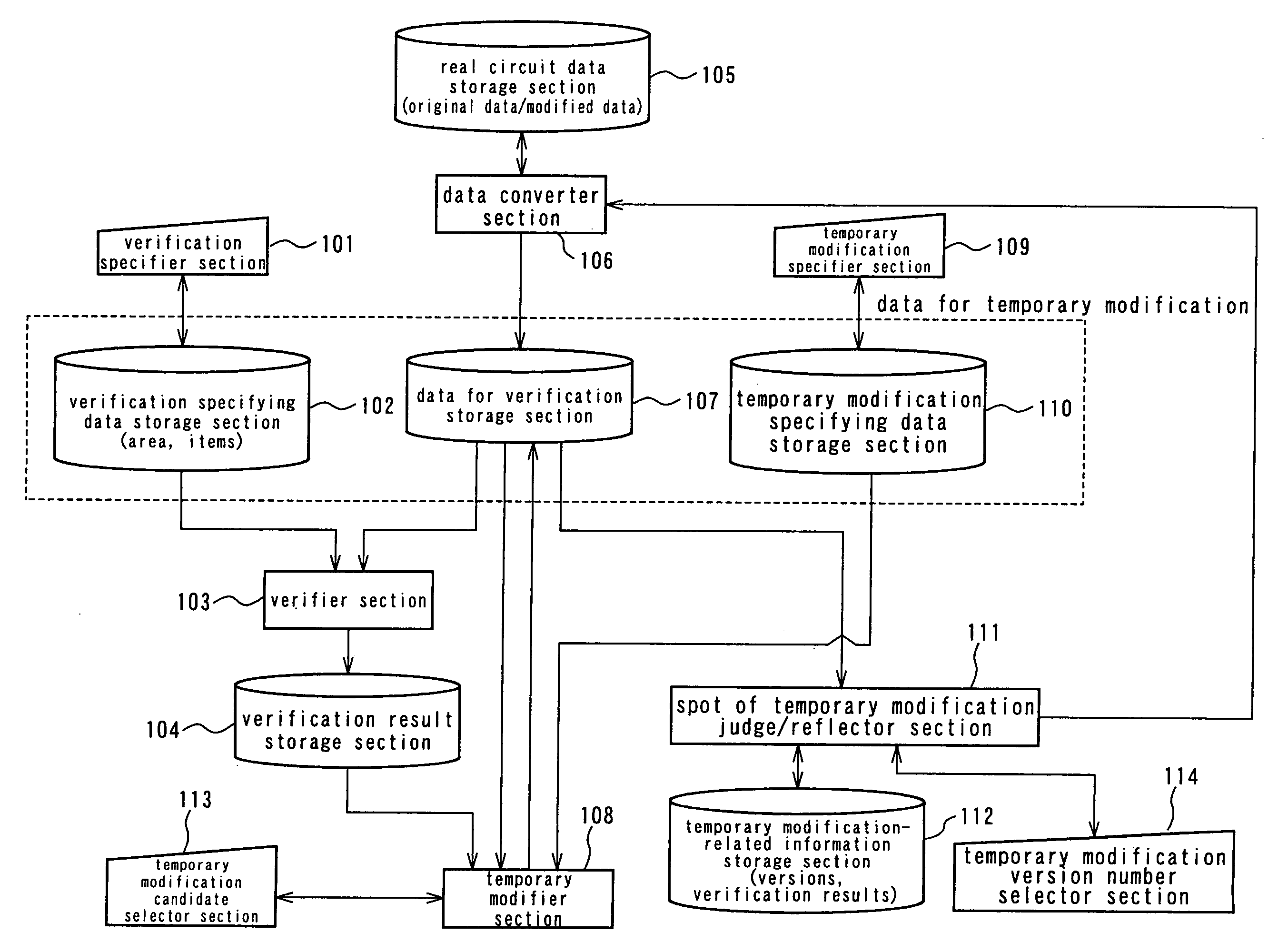
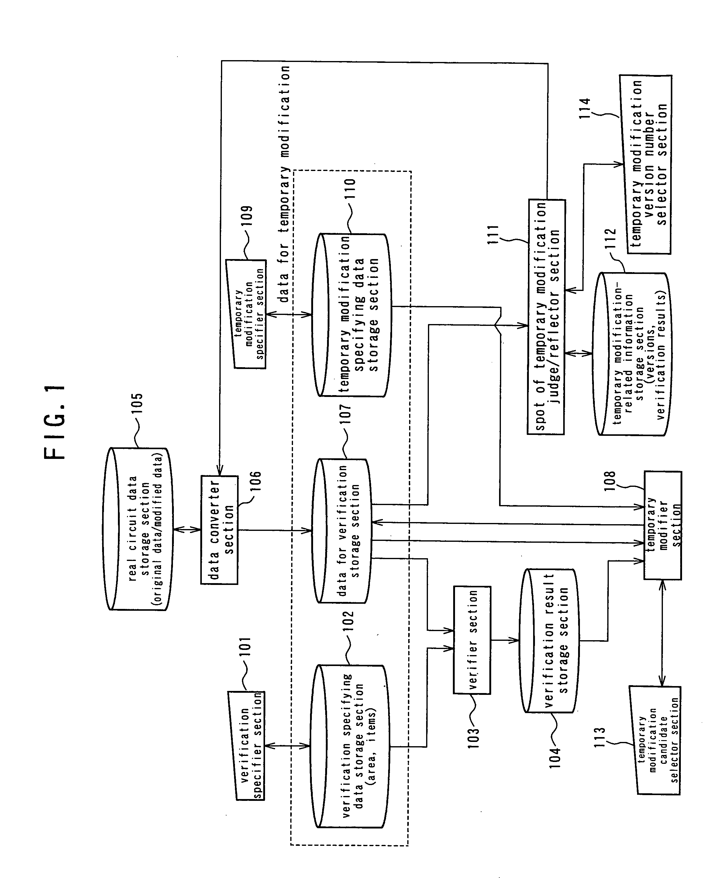
[0063]FIG. 1 is a schematic functional block diagram of an embodiment of logic verification device according to the invention, showing the entire configuration thereof.

[0064]This embodiment of logic verification device comprises a verification specifier section 101, a verification specifying data storage section 102, a verifier section 103, a verification result storage section 104, a real circuit data storage section 105, a data converter section 106, a data for verification storage section 107, a temporary modifier section 108, a temporary modification specifier section 109, a temporary modification specifying data storage section 110, a spot of temporary modification judge / reflector section 111, a temporary modification-related information storage section 112, a temporary modification candidate selector section 113, ...


PUM


Abstract

A logic verification device, a logic verification method and a logic verification computer program that can reduce the number of steps involved in designing a logic circuit particularly when the designed logic circuit is subjected to logic verification and modification at the spot where an error is detected. The logic verification device comprises a data converter section adapted to convert real circuit data to be processed for designing a logic circuit into data for verification to be processed for logic verification and vice versa, a verifier section adapted to operate for logic verification of said data for verification and a temporary modifier section adapted to acquire the result of verification of said verifier section and the modification candidate data corresponding to the result of verification of said verifier section and pre-selected as candidate data for modification of said data for verification and modify said data for verification on the basis of said acquired result of verification and said acquired modification candidate data.

Description

BACKGROUND OF THE INVENTION[0001]1. Field of the Invention[0002]This invention relates to a logic verification device, a logic verification method and a logic verification computer program.[0003]2. Description of the Related Art[0004]In conventional operations of designing logic circuits by means of CAD techniques, the designed logic circuit is logically verified in order to eliminate logic design errors that can intervene during the design procedures by mistake.[0005]If an error is detected as a result of logic verification, the designer looks into the cause of the error and corrects the designed logic circuit so as to remove the cause of the detected error.[0006]Generally, the data to be processed in the operation of designing a logic circuit and correcting it (hereinafter referred to as real circuit data) and the data to be processed in the operation of logic verification (hereinafter referred to as data for verification) are different from each other in terms of data format. The...

Claims


Application Information

Patent Timeline
Patent Type & Authority Patents(United States)
IPC IPC(8): G06F17/50
CPCG06F17/5022G06F30/33
Inventor YAMASAKI, JUNYAMAEDA, SUMIKOTAKEYAMA, KENYAMAKINO, YUKIO
Owner FUJITSU LTD
Why Eureka
Try Eureka