High performance silicon condenser microphone with perforated single crystal silicon backplate

a silicon condenser microphone and silicon backplate technology, applied in the direction of piezoelectric/electrostrictive transducers, transducer types, electrostatic transducers of semiconductor electrostatic transducers, etc., can solve the problem that the silicon microphone reported so far has not achieved sensitivity of more than 20 mv/pa, and the problem of large air gap requires a thick sacrificial layer

Inactive Publication Date: 2006-11-07
KNOWLES ELECTRONICS INC
View PDF9 Cites 46 Cited by
  • Summary
  • Abstract
  • Description
  • Claims
  • Application Information

AI Technical Summary

Benefits of technology

[0020]A principal object of the present invention is to provide an effective and very manufacturable method of fabricating a silicon condenser microphone having high sensitivity and low noise.
[0021]Another object of the invention is to provide a silicon condenser microphone design having high sensitivity and low noise.
[0023]Yet another object of the invention is to provide a method for fabricating a silicon condenser microphone using buckling of a composite diaphragm to prevent stiction in a wet release process.

Problems solved by technology

However, the large diaphragm requires a large span of anchored supports and correspondingly a large backplate.
Also, a large air gap requires a thick sacrificial layer.
These present major difficulties in / silicon micro-machining processes.
Due to constraints of material choices and intrinsic stress issues in silicon micro-machining, the silicon microphones reported so far have not achieved sensitivity of more than 20 mV / Pa.
However, none of the silicon condenser microphones mentioned above has been reported to achieve sensitivity above 20 mV / Pa.
However, this microphone must be fit onto a bulky pre-amplifier and requires a polarization voltage of 200 V.

Method used


Image

  • High performance silicon condenser microphone with perforated single crystal silicon backplate
  • High performance silicon condenser microphone with perforated single crystal silicon backplate
  • High performance silicon condenser microphone with perforated single crystal silicon backplate

Examples


Embodiment Construction

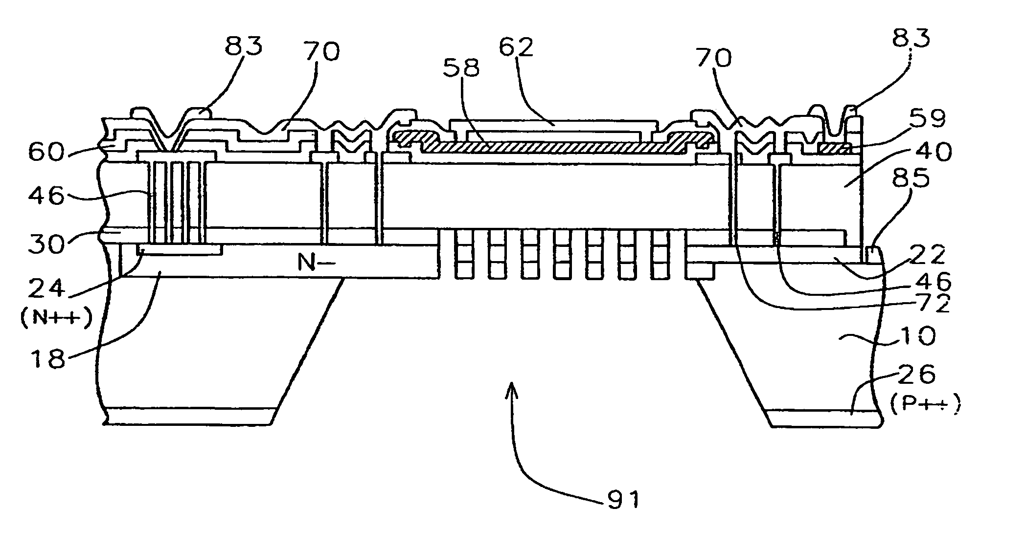
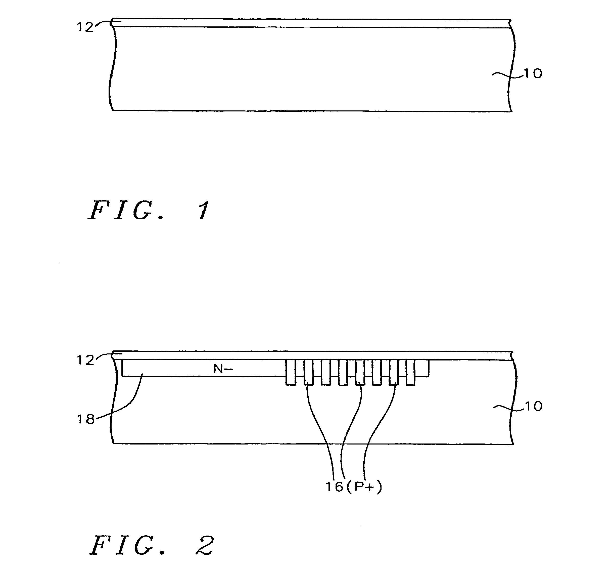
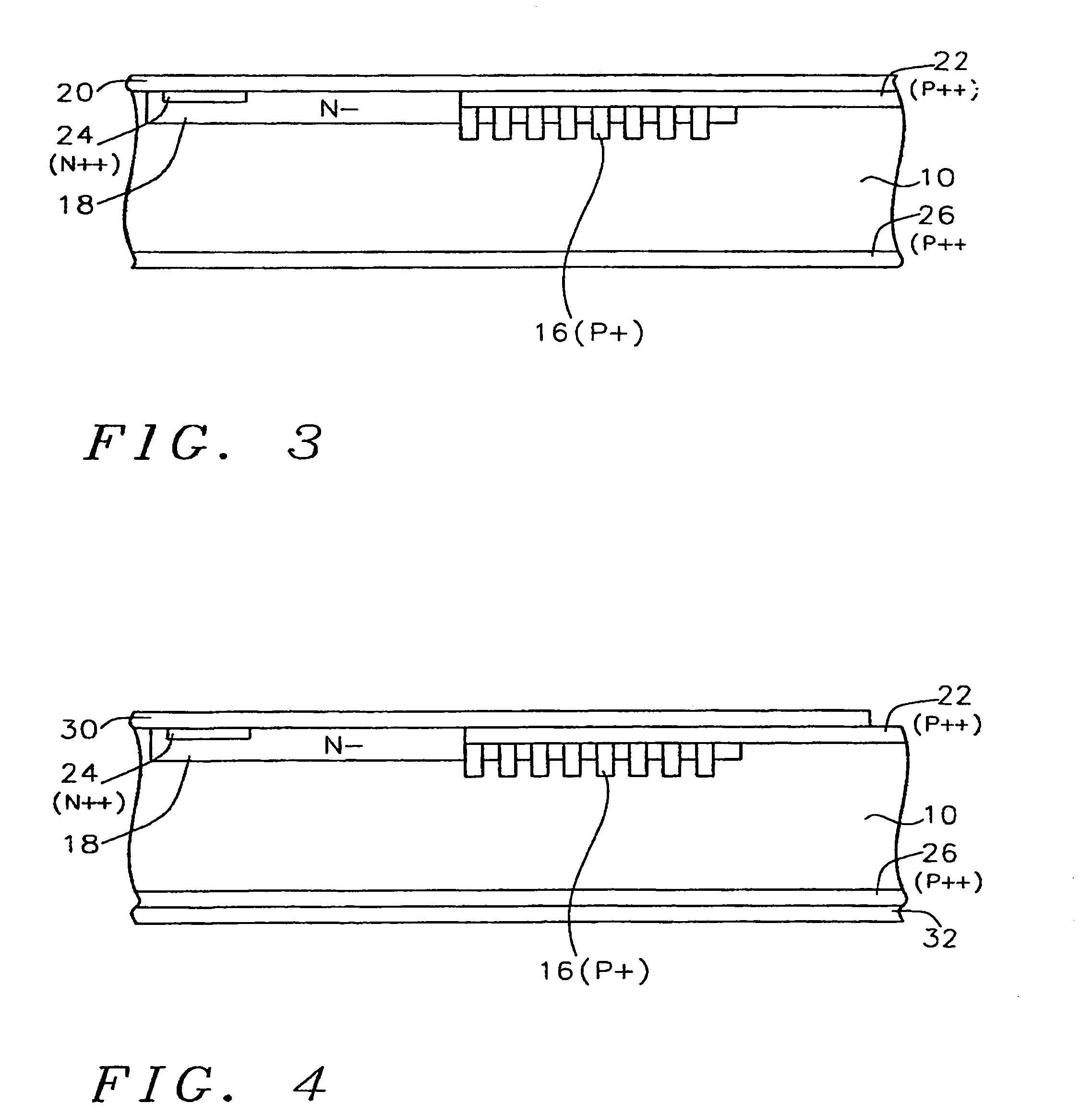
[0033]The present invention discloses a novel design and process for making a silicon condenser microphone. Referring now more particularly to FIG. 1, there is shown a semiconductor substrate 10, preferably composed of P-doped monocrystalline silicon. A thermal oxide layer 12 is grown on the surface of the substrate to a thickness of between about 270 and 330 Angstroms.

[0034]Referring now to FIG. 2, P+ implants 16 are made through a mask, not shown. These implanted regions 16 will form acoustic holes on the backplate in the later selective silicon etching process. The P+ implant condition must ensure the acoustic hole size at a desired backplate thickness. Now, an N− implanted region 18 is formed using a second mask, not shown. The N− implant condition must ensure a low stress backplate so that the backplate will not deform after the release process at the end of the fabrication process. The implanted ions are driven in to a depth of about 10 microns, which is the depth of the N− re...


PUM

PropertyMeasurementUnit
thicknessaaaaaaaaaa
thicknessaaaaaaaaaa
diameteraaaaaaaaaa

Abstract

A silicon condenser microphone is described. The silicon condenser microphone of the present invention comprises a perforated backplate comprising a portion of a single crystal silicon substrate, a support structure formed on the single crystal silicon substrate, and a floating silicon diaphragm supported at its edge by the support structure and lying parallel to the perforated backplate and separated from the perforated backplate by an air gap.

Description

BACKGROUND OF THE INVENTION[0001](1) Field of the Invention[0002]The invention relates to a method of manufacturing a silicon condenser microphone, and more particularly, to a method of manufacturing a high performance silicon condenser microphone using a silicon micro-machining process.[0003](2) Description of the Prior Art[0004]Silicon condenser microphones have long been an attractive research and development subject. Various microphone designs have been invented and conceptualized by using silicon micro-machining technology. Despite various structural configurations and materials, the silicon condenser microphone consists of four basic elements: a movable compliant diaphragm, a rigid and fixed backplate (which together form a variable air gap capacitor), a voltage bias source, and a pre-amplifier. These four elements fundamentally determine the performance of the condenser microphone. In pursuit of high performance; i.e., high sensitivity, low bias, low noise, and wide frequency...

Claims


Application Information

Patent Timeline
Patent Type & Authority Patents(United States)
IPC IPC(8): H01L21/00H04R25/00H04R19/00
CPCH04R19/005Y10T29/49005
Inventor WANG, ZHEZHANG, QINGXINFENG, HANHUA
Owner KNOWLES ELECTRONICS INC
Why Eureka
Try Eureka