Image processing apparatus having an image correction circuit and its processing method

Inactive Publication Date: 2006-11-07
CANON KK
View PDF21 Cites 74 Cited by
  • Summary
  • Abstract
  • Description
  • Claims
  • Application Information

AI Technical Summary

Benefits of technology

[0011]It is an object of the present invention to provide an image processing apparatus which can gen

Problems solved by technology

An image sensing element such as a CCD sensor, CMOS sensor, or the like has defective pixels called white spots with abnormally large dark currents, which often deteriorate the image performance of the image sensing element.
However, a high-end digital camera must provide high-quality images even under severe image sensing conditions such as high ISO (International Organization for Standardization) speed rating, long shutter time, and high temperature.
However, in such case, information of pixels which do not have so large dark currents and can be used without correction is discarded, thus narrowing down an effective dynamic range.
Furthermore, in Japanese Patent Laid-Open No. 11-239298, white spots (white scratches) which increase/decrease in accordance with the exposure time merely undergo defect correction in accordance with the exposure time, a

Method used


Image

  • Image processing apparatus having an image correction circuit and its processing method
  • Image processing apparatus having an image correction circuit and its processing method
  • Image processing apparatus having an image correction circuit and its processing method

Examples


Example

[0043]A preferred embodiment of the present invention will be described hereinafter with reference to the accompanying drawings.

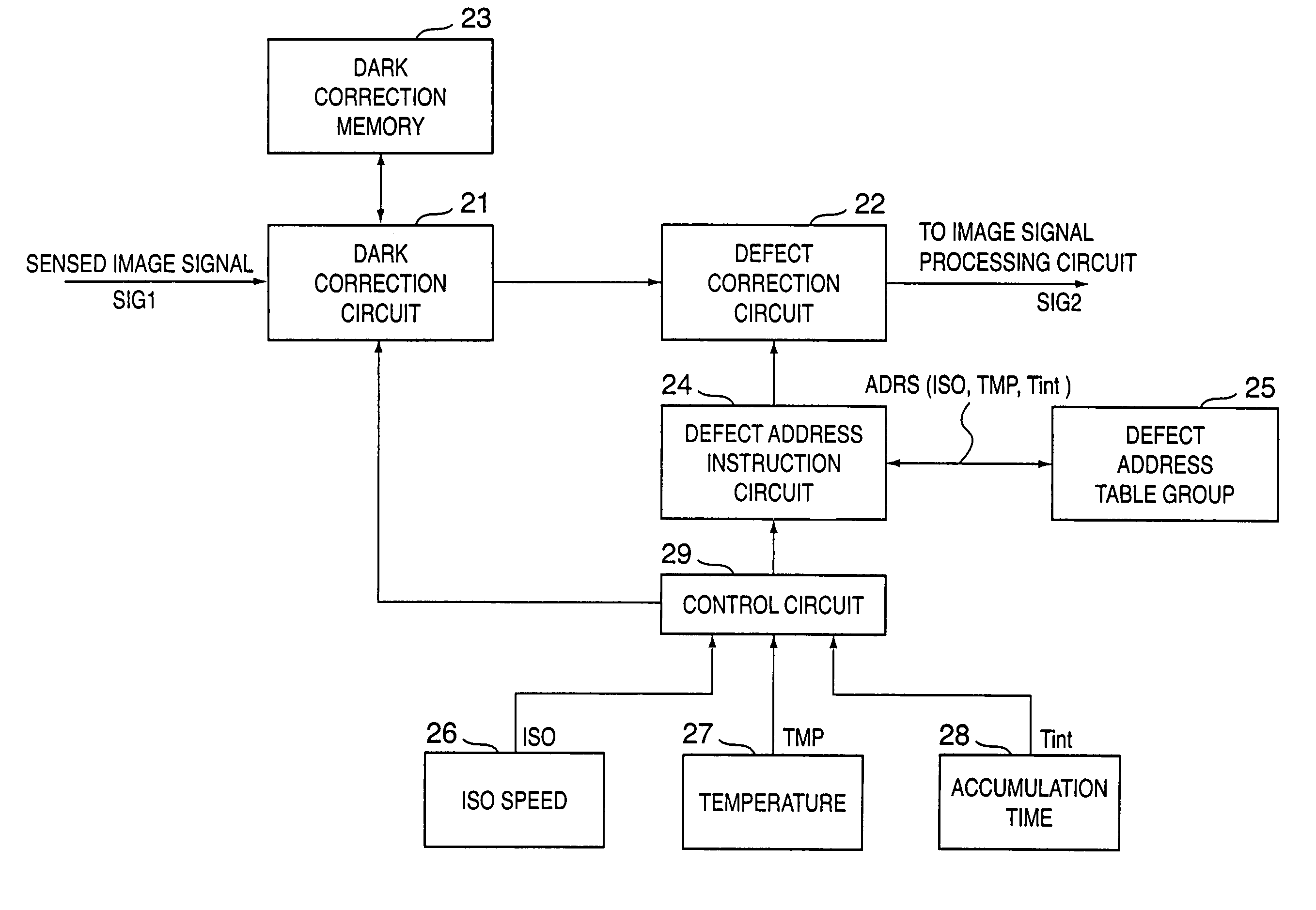
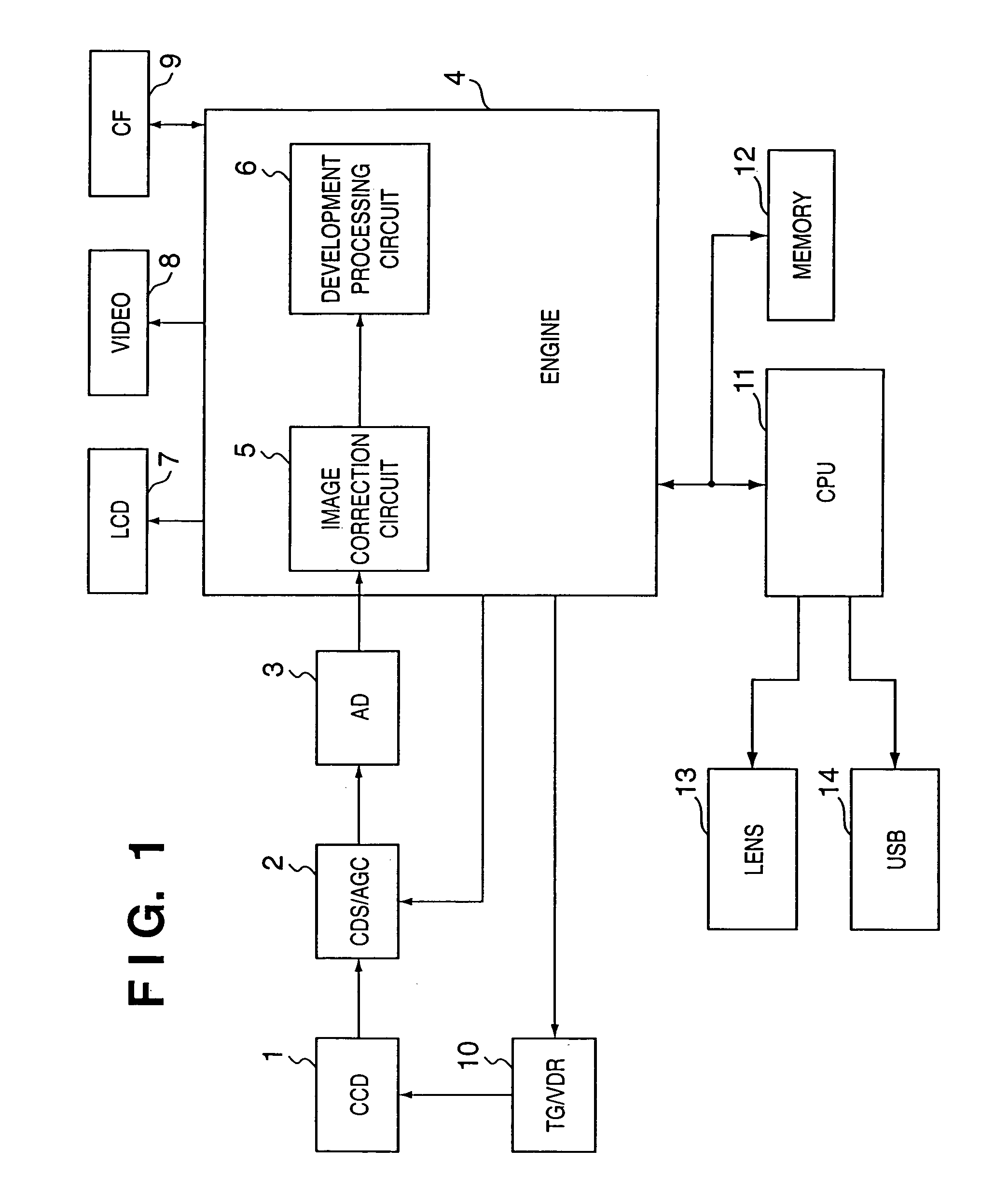
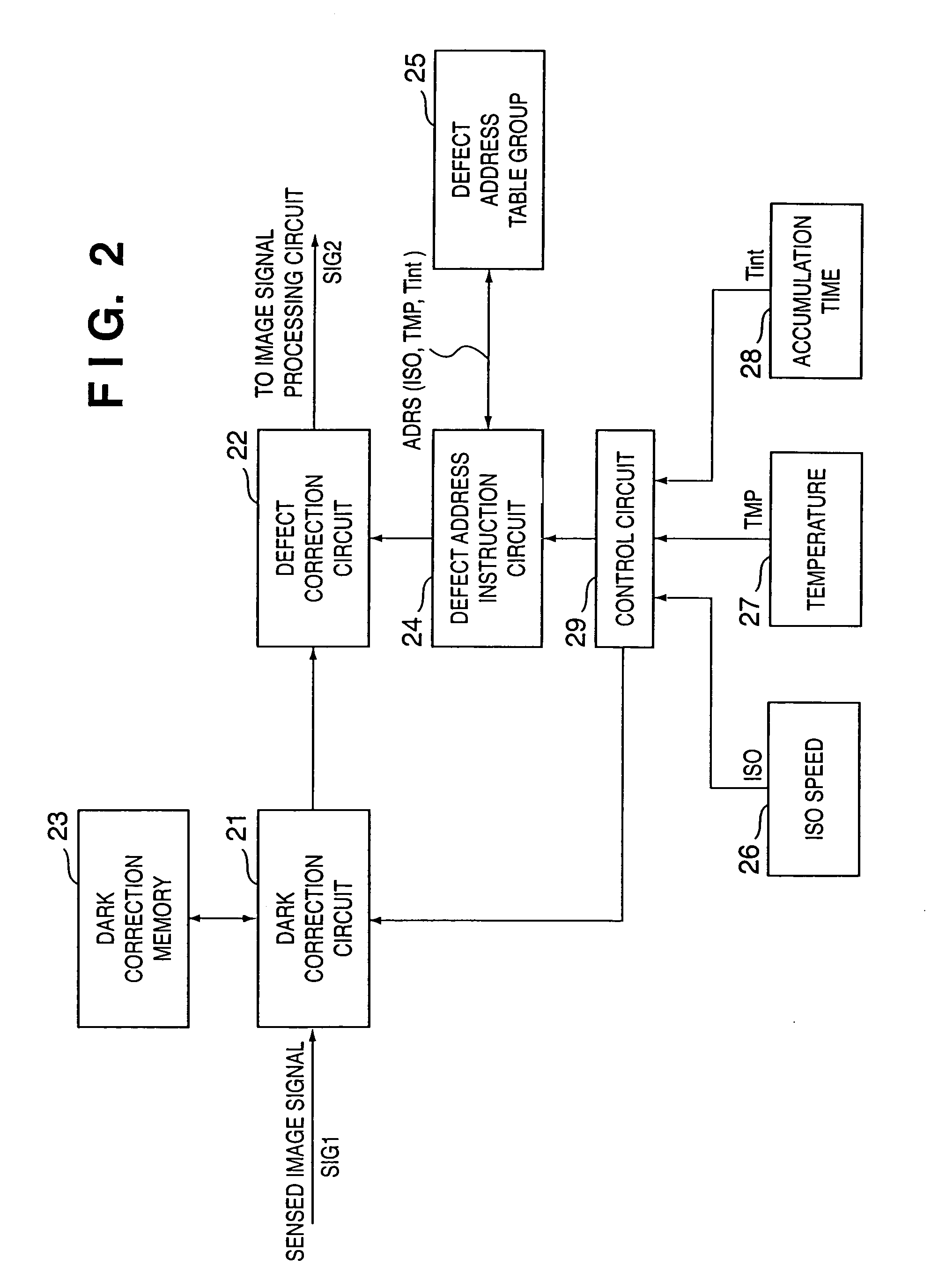
[0044]FIG. 1 is a block diagram of a digital camera (image processing apparatus) using an image sensing element having a plurality of photoelectric conversion units, such as a CCD sensor, CMOS sensor, or the like. An output from a CCD 1 as an image sensing element having a plurality of photoelectric conversion units undergoes noise reduction and gain adjustment in a CDS / AGC 2, and the output from the CDS / AGC 2 is converted from an analog signal into a digital signal by an A / D converter 3. The digital signal is input to an engine 4 as a digital signal processing IC.

[0045]The engine 4 includes an image signal correction circuit 5 and development processing circuit 6. An image signal input to the engine 4 undergoes dark correction and defect correction in the image signal correction circuit 5, and then undergoes a development process such as a color interpolat...


PUM


Abstract

An image processing apparatus for processing an image sensed by an image sensing element such as a CCD sensor includes a dark correction circuit for making dark correction of the image, a defect correction circuit for correcting a defective pixel in the image using other pixels, and a controller for controlling the shares of dark correction by the dark correction circuit and defect correction by the defect correction circuit on the basis of information which pertains to image sensing such as an ISO speed, temperature, and accumulation time.

Description

FIELD OF THE INVENTION[0001]The present invention relates to an image processing apparatus for correcting any defects of an image sensing element, and its processing method.BACKGROUND OF THE INVENTION[0002]An image sensing element such as a CCD sensor, CMOS sensor, or the like has defective pixels called white spots with abnormally large dark currents, which often deteriorate the image performance of the image sensing element. By correcting such defective pixels by defect correction, the yield of expensive image sensing elements can be improved.[0003]However, a high-end digital camera must provide high-quality images even under severe image sensing conditions such as high ISO (International Organization for Standardization) speed rating, long shutter time, and high temperature. The ISO speed indicates the sensitivity of a film to light, and is indicated by a converted value in a digital camera.[0004]For this purpose, defective pixels under such worst conditions (i.e., high ISO speed...

Claims


Application Information

Patent Timeline
IPC IPC(8): H04N9/64H01L29/762G06T1/00H01L21/339H01L27/146H01L27/148H04N1/401H04N5/335H04N5/355H04N5/367H04N5/372H04N5/374H04N5/378H04N9/07
CPCH04N5/2176H04N25/63
Inventor HARADA, YOSHIHITO
Owner CANON KK
Why Eureka
Try Eureka