Low power, high speed read method for a multi-level cell DRAM

a multi-level cell, low power, read-only technology, applied in the field of memory devices, can solve the problems of low noise margin, unstable globe reference voltage, low noise margin, etc., and achieve the effect of reducing the circuit complexity of the write process

Active Publication Date: 2006-11-07
LIU BO
View PDF8 Cites 56 Cited by
  • Summary
  • Abstract
  • Description
  • Claims
  • Application Information

AI Technical Summary

Benefits of technology

[0010]In the present invention, a method has been designed, which has the benefits of using conventional reference voltage levels, increasing the speed of multi-level DRAM and also decreasing the power consumption of DRAM, specially for a three level DRAM.
[0019]The write operation can also be realized by using the restore circuit and ASA and reduce the circuit complexity of the write process.
[0020]Since the first sense operation can start after word line reaches Vcc / 2 and can output data immediately after the first read operation, so the speed is faster than conventional DRAM at the first read operation. The second sense operation starts after word line reaches Vccp and then ASA generates the data, also the write back circuit and ASA restore the data back memory cells at this stage. The second sense operation is also faster than conventional DRAM since word line does not need to rise from 0 to Vccp but from Vcc / 2 to Vcc. Both latch based sense amplifier and differential based sense amplifier can be used in this scheme.

Problems solved by technology

This method can read 2 bit data out at one time and fast, but the disadvantage of this scheme is also very obvious that it need three sense amplifiers, more switches and control circuit for sub bit line and a worst disadvantage is that it's susceptibility to sense errors with unstable globe reference voltage and small noise margin.
And even this scheme is faster comparing to the following scheme, it still need more switching operations and decoding operations, these operation make this scheme still slower than most conventional DRAM.
The disadvantage of this scheme is that it still use 2 sense amplifier and has lots of control and switches circuit for sub bit line concept, it also has the problem of much low noise margin compare to conventional DRAM because needs more reference voltage levels.
Furthermore, the speed is even slower than Furuyama's scheme.
Nevertheless, this scheme is limited by the prior scheme's low noise margin problem of multi-level DRAM.
The disadvantage for this scheme is that it has to read out the data (0 or 1 or 2) before it can do the decoding.

Method used


Image

  • Low power, high speed read method for a multi-level cell DRAM
  • Low power, high speed read method for a multi-level cell DRAM
  • Low power, high speed read method for a multi-level cell DRAM

Examples


Embodiment Construction

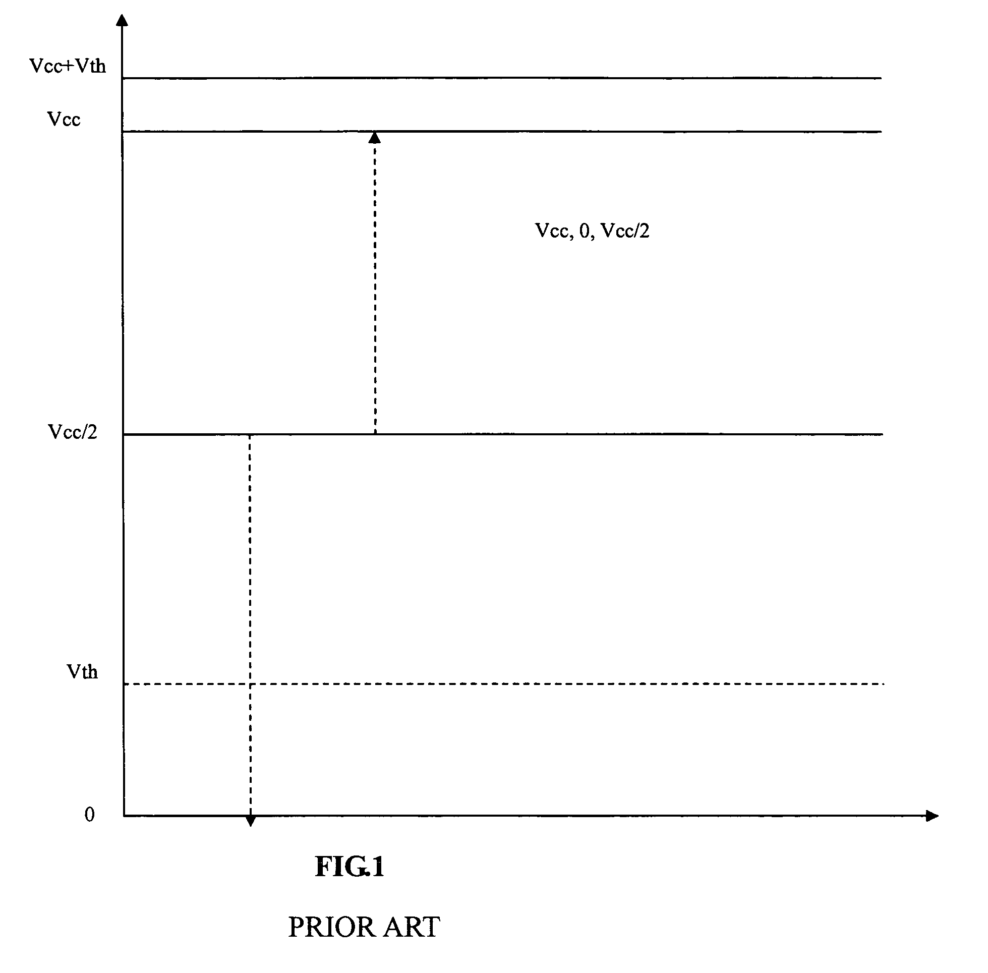
[0031]In order to store more than one bit in a single memory cell capacitor, the cell capacitor must store more than 2 voltage levels, specifically, for storing 1.5 bits per cell, cell capacitor should store 3 voltage levels such as GROUND (0), Vcc / 2 any Power supply (Vcc) as shown in FIG. 1.

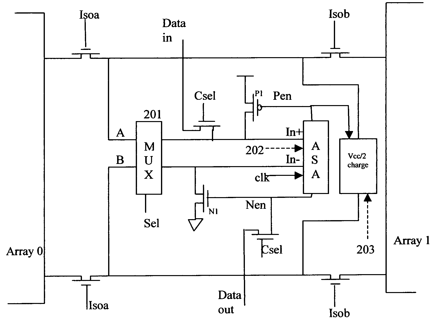
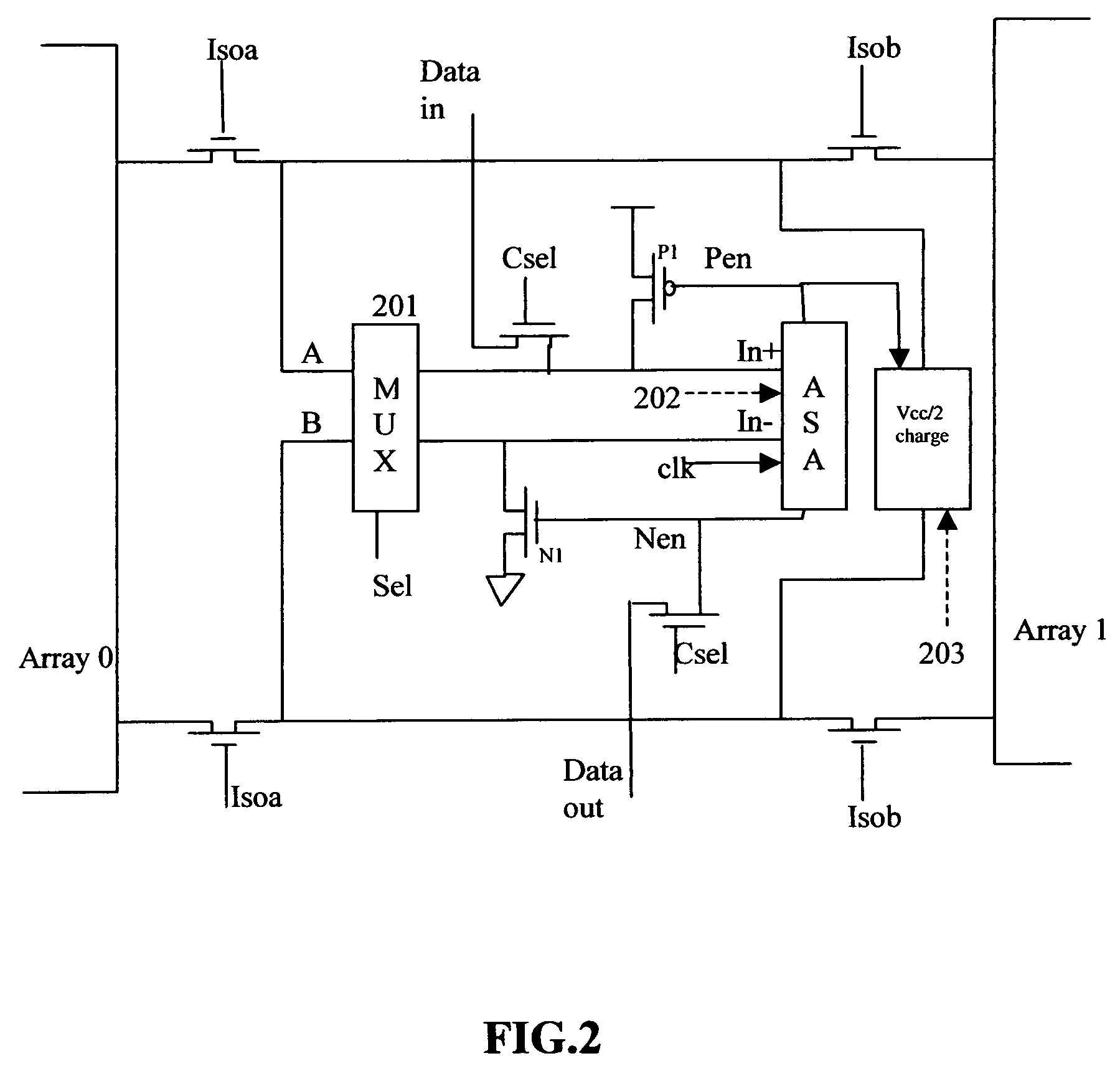
[0032]The reference bit line and reference memory cell capacitor are always charge to vcc / 2. Before a sensing operation happens, the bit line capacitor voltage charged to Vcc / 2, then word line voltage increases to Vccp, depending on stored voltage, the bit line voltage may increase, decrease, or unchanged. At the first sense operation, the accessed bit line connected to the input In− of ASA, at the second sense operation, the accessed bit line connected to the input In+ of ASA. This configuration is controlled by a multiplex whose input is Sel from an exclusive or gate as shown in FIG. 3B. The En signal to the XOR gate tells multiplex which bit line, A or B, is the accessed bit line, so the mult...


PUM


Abstract

A method of storing, sensing and restoring three voltage levels (1.5 bit per cell) of a plurality of memory cells in Dynamic random access memory is disclosed. An asymmetrical sense amplifier, ASA, together with a 2 to 2 multiplex, will be used to detect the voltage difference on the bit lines and transfer the voltage difference to digital data. ASA is designed to have one input stronger than the other input. The multiplex is controlled by a signal so that the connection between bit line pair and two inputs of ASA is switched at different time and logical address. Other transistors and circuits are also used to store and restore the voltage levels into memory cells. Coding algorithms are used to get fast read speed of this multi-level cell DRAM.

Description

CROSS-REFERENCE TO RELATED APPLICATION[0001]Claim the benefit of one prior filed copending provisional application. application Ser. No. 60 / 601,819 Filed Date: Aug. 16, 2004 Inventor: BO LIUSTATEMENT REGARDING FEDERALLY SPONSORED RESEARCH OR DEVELOPMENT[0002]Not ApplicableREFERENCE TO SEQUENCE LISTING, A TABLE OR A COMPUTER PROGRAM LISTING COMPACT DISK APPENDIX[0003]Not ApplicableBACKGROUND OF THE INVENTION[0004]This invention relates generally to memory devices and particularly to dynamic random memory device with multilevel memory cells. A multi-level cell DRAM can store more than two voltage levels in the memory and thus can store more than 1 bit per cell. Although store four voltage levels in memory cells can achieve more density efficiency, in practice store three-level voltage in memory cells is easier due to the noise margin problem in multi-level DRAM.[0005]Suggested Classification: 365 / 149; 365 / 189; 365 / 168; 365 / 94[0006]T. Furuyama et al (“Furuyama”) in an article titled “A...

Claims


Application Information

Patent Timeline
Patent Type & Authority Patents(United States)
IPC IPC(8): G11C11/54G11C7/02
CPCG11C11/4076G11C11/4091G11C11/565G11C7/06
Inventor LIU, BO
Owner LIU BO
Why Eureka
Try Eureka