Method and apparatus for reticle inspection using aerial imaging

Inactive Publication Date: 2006-11-07
APPLIED MATERIALS INC
View PDF37 Cites 61 Cited by
  • Summary
  • Abstract
  • Description
  • Claims
  • Application Information

AI Technical Summary

Benefits of technology

[0023]In view of the foregoing, it is one feature of the present invention to provide an inspection system that provides more complete information on the properties of the photolithographic mask. Par

Problems solved by technology

The major limitations on the resolution of the image that can be projected on the photoresist are created by the illuminating light diffraction effects on the features of the mask and the limitations on the quality of the mask itself.
Therefore, mask inspection tools are needed to detect various defects in the masks that can potentially reduce the microelectronic circuit fabrication yields.
Because this method is expensive, time-consuming, and often inaccurate, it is uneconomical and inefficient.
The major drawback of this method is that it studies the physical structure of the mask independently of the optical image actually produced by the mask on the wafer.
Despite all the above advantages, the Zeiss/IBM system has limited application as a printability review station for a set of detected defects by other inspection systems.
The simulation process takes into account optical proximity effects due to the limited resolution of the optical exposure system and the proximity effects due to the photoresist etching during the mask manufacturing process.
Despite the above advances in the mask inspection technology, at the prese

Method used


Image

  • Method and apparatus for reticle inspection using aerial imaging
  • Method and apparatus for reticle inspection using aerial imaging
  • Method and apparatus for reticle inspection using aerial imaging

Examples


Embodiment Construction

[0034]Embodiments of the invention will now be described, by way of example only, with reference to the attached drawings.

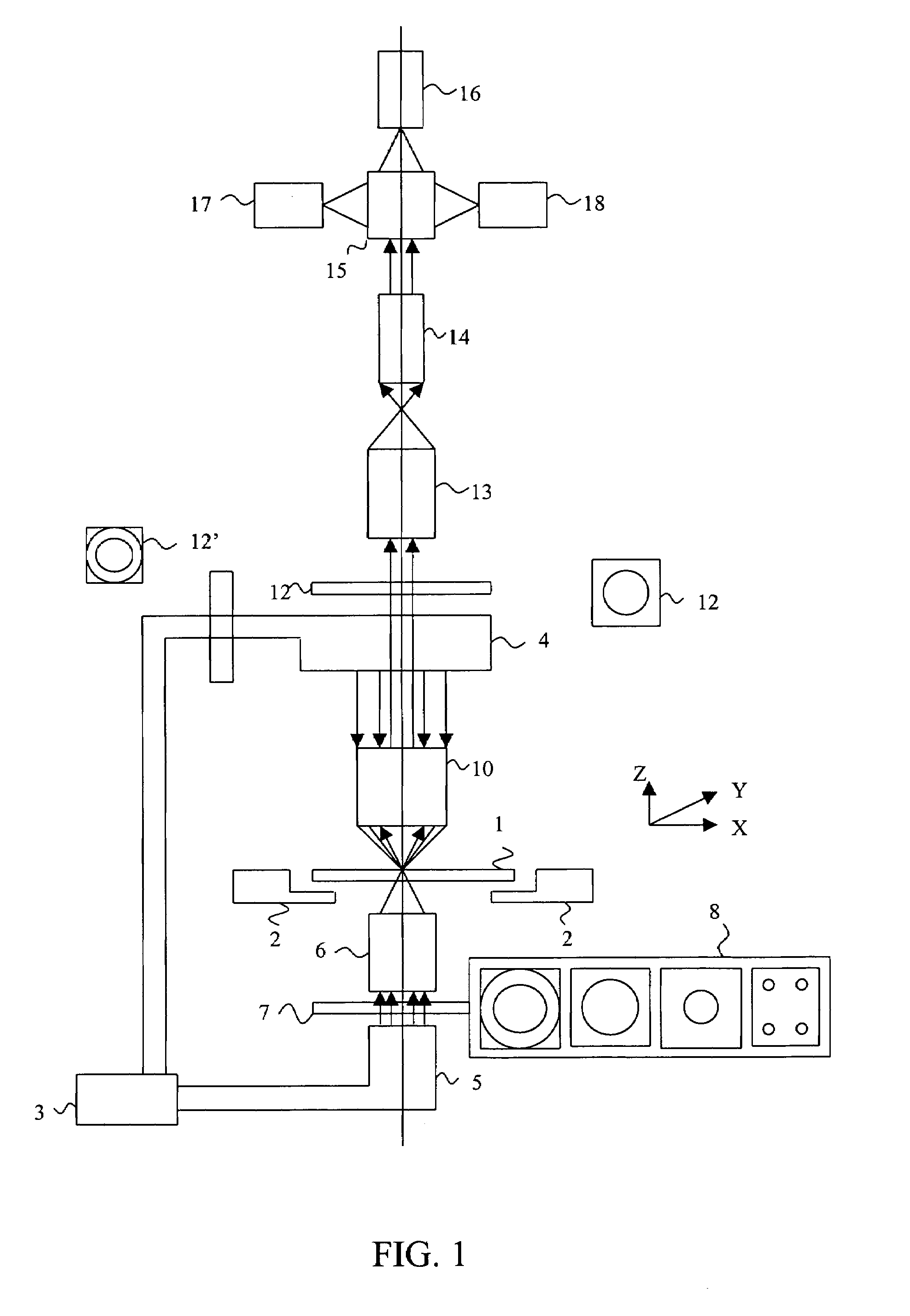
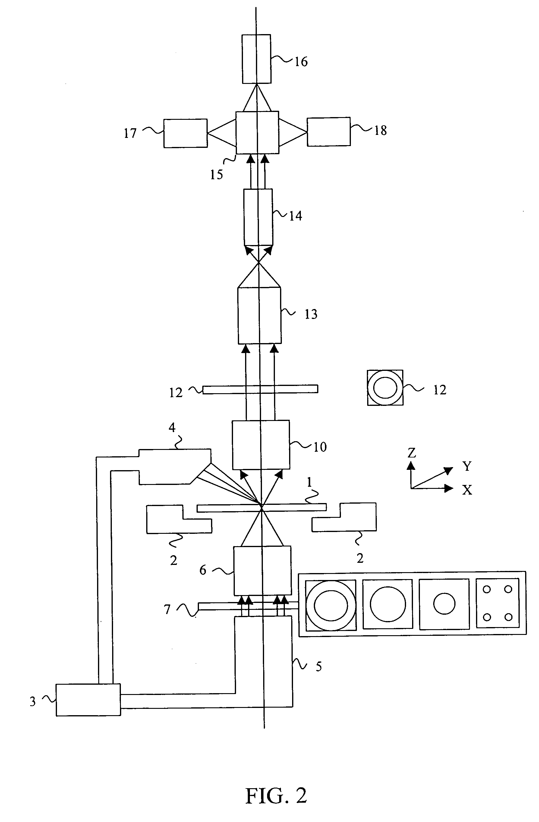
[0035]The system for defect detection according to the present invention is composed of three main modules: (1) a scanner module; (2) a defect detection image processing hardware module; and (3) a post process and review station. The scanner module scans the reticle and acquires aerial images of the reticle in transmitted light at a plurality of focal planes, preferably three, and dark field images of the reticle in reflected light at one focal plane. By properly adjusting the apertures of the illuminating and imaging parts of the optical system, the NA and the coherence factor are adjusted. The optical system of the scanner module simulates the behavior of an optical exposure system and, as a result, the acquired transmission light aerial images are optically equivalent to those produced on the photoresist under a given set of exposure conditions. The image proc...


PUM


Abstract

A reticle inspection system for inspecting reticles can be used as an incoming inspection tool, and as a periodic and pre-exposure inspection tool. Mask shops can use it as an inspection tool compatible to their customers, and as a printable error detection tool. The inventive system detects two kinds of defects: (1) line width errors in the printed image; (2) surface defects. The line width errors are detected on the die area. The detection is performed by acquiring the image of the reticle under the same optical conditions as the exposure conditions, (i.e. wavelength, numerical aperture, sigma, and illumination aperture type) and by comparing multiple dies to find errors in the line width. Surface defects are detected all over the reticle. The detection of surface defects is performed by acquiring transmission and dark-field reflection images of the reticle and using the combined information to detect particles, and other surface defects.

Description

[0001]This is a divisional of application Ser. No. 09 / 417,518 filed Oct. 13, 1999, the disclosure of which is incorporated herein by reference.BACKGROUND OF THE INVENTION[0002]1. Field of the Invention[0003]This invention relates to techniques for inspecting reticles that are used in fabricating microelectronic devices through a microphotolithographic process. Particularly, the present invention relates to a method and an apparatus for detecting variations in line width and other defects that would be printed on the wafer using such reticles by emulating the operation of a specific photolithography tool in which this reticle is to be used. The invention is embodied in a method and an apparatus that can readily be used for inspecting reticles in the industrial environment.[0004]2. Description of the Background Art[0005]Modern microelectronic devices are commonly produced using a photolithographic process. In this process, a semiconductor wafer is first coated with a layer of photores...

Claims


Application Information

Patent Timeline
IPC IPC(8): G06K9/00G01B11/24G01N21/956G03F1/00G03F7/20H01L21/027
CPCG03F7/701G03F7/70125G03F7/70616G03F7/70633G03F1/0092G03F1/84
Inventor KENAN, BOAZERAN, YAIRKARPOL, AVNERELYASAF, EMANUELTIROSH, EHUD
Owner APPLIED MATERIALS INC
Why Eureka
Try Eureka