

Insulated gate type semiconductor device and method for fabricating same
a semiconductor device and gate type technology, applied in the direction of semiconductor devices, electrical devices, transistors, etc., can solve the problems of increasing chip area, short circuit between body contact electrodes and source and drain electrodes, and inability to remove the parasite at the portion that cannot be solved, so as to prevent an increase of parasitic capacitance
- Summary
- Abstract
- Description
- Claims
- Application Information
AI Technical Summary
Benefits of technology
Problems solved by technology
Method used
Image

Examples
first embodiment
[0089]Here, the explanation will be given of the process of production of an SOI-MOSFET according to the present invention with reference to FIG. 2 to FIG. 6. To simplify the explanation, the explanation will be given of the process of production of an n-channel type MOSFET.
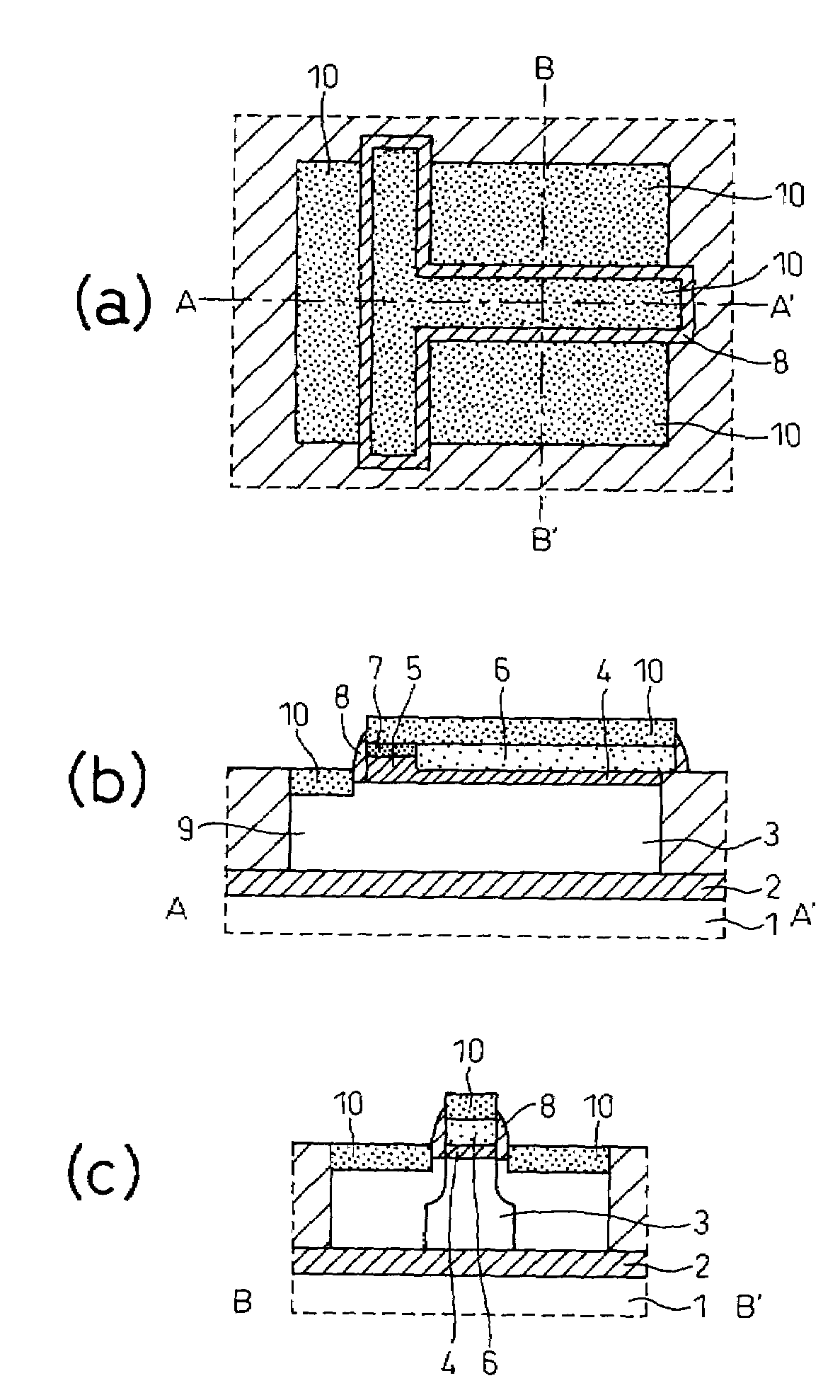
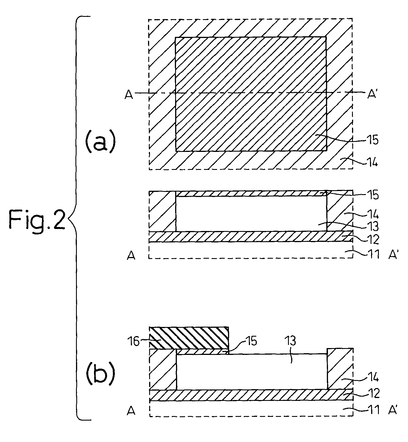
[0090]In FIG. 2(a), the top view is a plan view, while the bottom views are sectional views along the one-dot chain line connecting A–A′ of the plan view.
[0091]First, oxygen ions are implanted to a predetermined depth in the silicon substrate 11, then heat treatment is performed to convert the oxygen ion implanted region to SiO2 and form the substrate isolation oxide film 12. Next, by implanting boron ions in the surface of the substrate, a p-type silicon layer 13 is formed.
[0092]Next, an element isolation oxide film 14 is formed around the element formation region using the STI method. Next, the surface of the p-type silicon layer 13 is heat oxidized to form the gate insulating film 15.
[0093]Next, in FIG. 2(b), ...
second embodiment
[0113]Next, an explanation will be made of the process of production of an SOI-MOSFET according to the present invention with reference to FIG. 7 and FIG. 8.
[0114]First, in FIG. 7(a), in exactly the same way as the first embodiment, the steps until FIG. 5(f) are carried out to form the body contact region 30, then the resist pattern 28 is removed to obtain the structure of FIG. 7(a).
[0115]Next, in FIG. 7(b), this is dry etched, using the resist pattern 33 having an opening of a shape corresponding to the separator 21 as a mask, to thereby selectively remove only the separator 21.
[0116]Next, in FIG. 7(c), the resist pattern 33 is removed, then the reminder is washed. Next, a cobalt film 31 is deposited over the entire surface using the sputtering method.
[0117]In the washing step, since the thick portion 18 is present at the removed part of the separator 21, the SiO2 film at the removed part will not be removed by etching to expose the p-type silicon layer. Therefore, in that portion,...
third embodiment
[0124]Next, an explanation will be given of the process of production of an SOI-MOSFET of the present invention with reference to FIG. 9 to FIG. 12.
[0125]First, in FIG. 9(a), oxygen ions are implanted to a predetermined depth in the silicon substrate 11, the heat treatment is performed to convert the oxygen ion implantation region to SiO2 and thereby form the substrate isolation oxide film 12. Next, boron ions are implanted in the surface to form the p-type silicon layer 41. Next, the underlying SiO2 film 42 and the SiN film 43 serving as the stopper in the chemical mechanical polishing (CMP) step are successively formed.
[0126]Next, in FIG. 9(b), this is dry etched, using the resist pattern 44 as a mask, to thereby form a shallow trench 45 for separating the body contact formation region and the other regions.
[0127]Next, in FIG. 9(c), the resist pattern 44 is removed, then the reminder is dry etched, using a newly provided resist pattern 46 as a mask, to form an element isolation tr...
PUM
 Abstract
Description
Claims
Application Information