Phase locked loop with adaptive loop bandwidth

a phase lock and adaptive technology, applied in the direction of pulse automatic control, electrical equipment, construction, etc., can solve the problems of less than optimal locking time period, variable operation characteristics, and difficulty in accurately adjusting and reproducing the value of series resistors, so as to improve the stability of the loop, reduce the area of the chip die, and the effect of fast locking ra

Inactive Publication Date: 2006-11-14
SAMSUNG ELECTRONICS CO LTD
View PDF8 Cites 13 Cited by
  • Summary
  • Abstract
  • Description
  • Claims
  • Application Information

AI Technical Summary

Benefits of technology

[0008]The present invention is directed to a semiconductor device that includes an adaptive phase locked loop with improved loop stability and a faster locking rate. In one embodiment, this is accomplished in a manner that does not require an additional second charge pump for loop stability, and therefore the resulting phase locked loop of the present invention consumes less chip die area. In another embodiment, multiple charge pumps are used and the resulting response time for locking is improved over that which can be achieved by conventional embodiments.

Problems solved by technology

This embodiment, however, is prone to process and temperature variation, which, in turn, can lead to variable operation characteristics.
In addition, the value of the series resistor is difficult to adjust and reproduce accurately.
While the configuration of FIG. 1 provides for a relatively stable phase locked loop operation, the current Ip that is provided by the first charge pump 12 is fixed, and therefore, the locking time period for the loop is less than optimal.
Also, the second charge pump 14 used in combination with the operational amplifier 16 to improve loop stability requires a large area of the chip die, leading to manufacturing inefficiencies.

Method used


Image

  • Phase locked loop with adaptive loop bandwidth
  • Phase locked loop with adaptive loop bandwidth
  • Phase locked loop with adaptive loop bandwidth

Examples


first embodiment

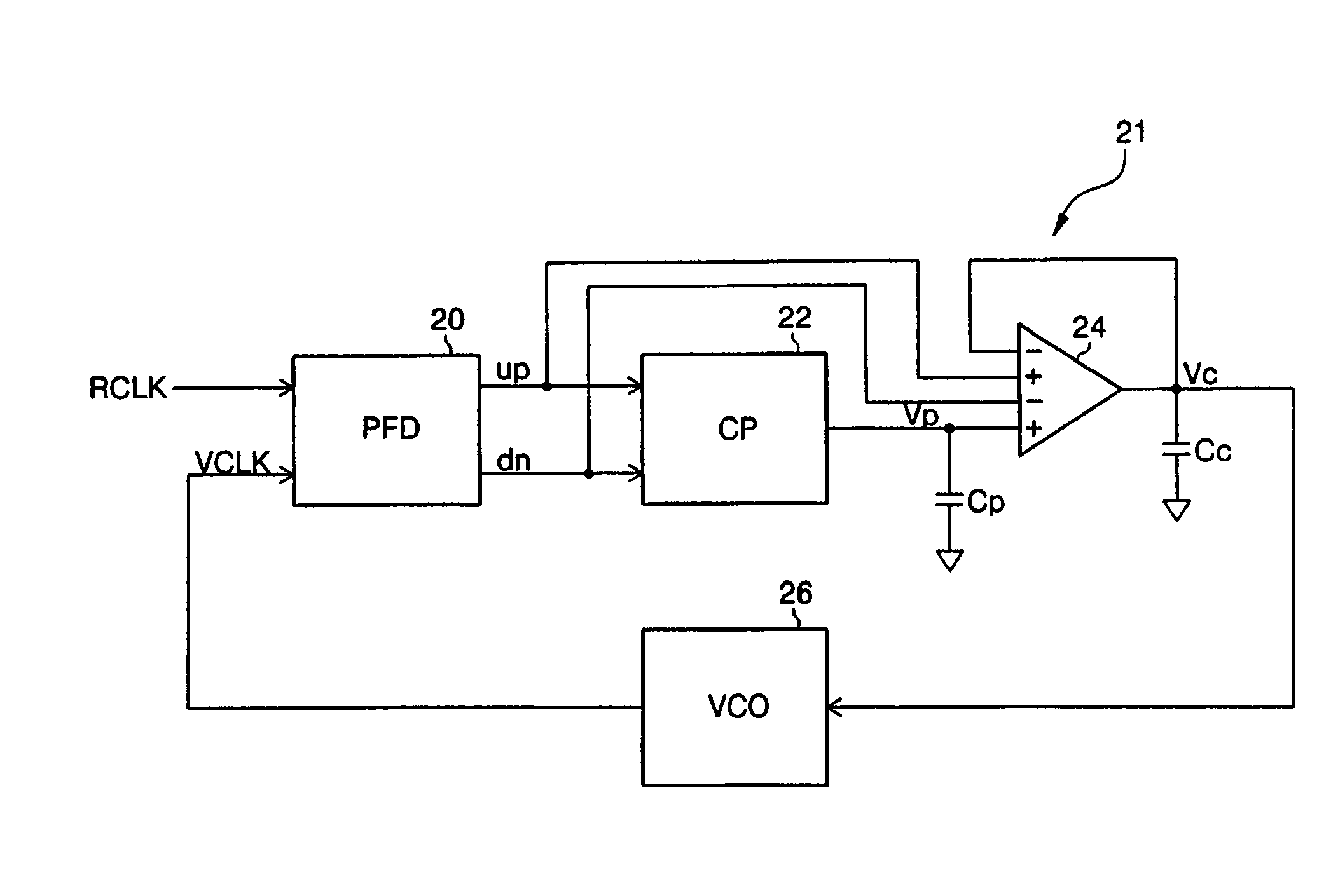
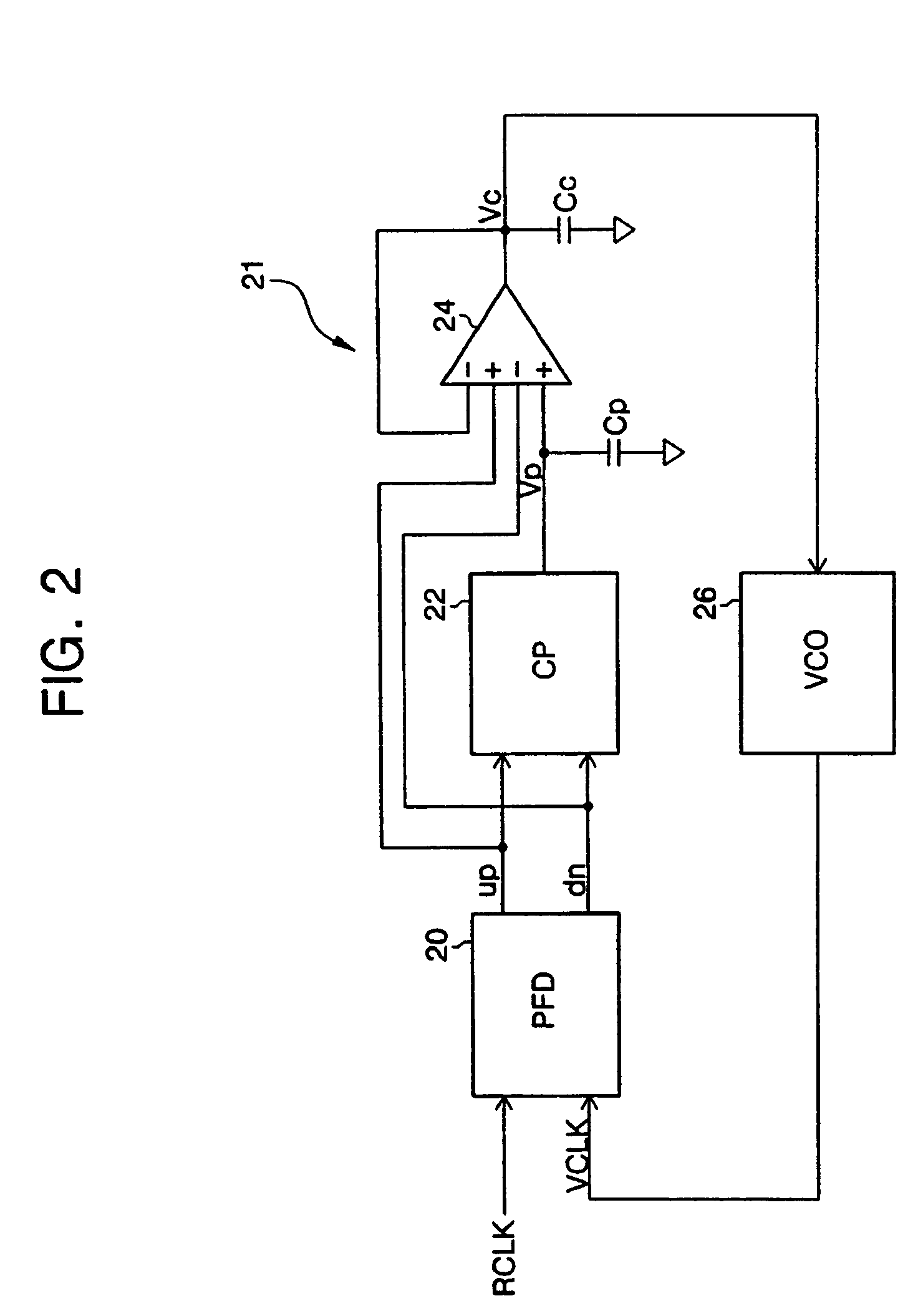
[0074]An advantage of the present first embodiment of the present invention lies in that the voltage Vc provided at the output of the operational amplifier 24 is provided solely by the operational amplifier 24 and thus, no additional charge pump is needed for this purpose.

[0075]FIG. 4A is a first timing diagram of signals of the phase locked loop of FIG. 2, in the case where the reference clock signal RCLK leads the feedback clock signal VCLK, in accordance with the present invention. At the rising edge of the RCLK signal, the up control signal up is activated by the phase frequency detector 20. With activation of the up control signal up, the first charge pump 22 causes the first charge pump signal Vp to charge the first capacitor Cp, and thus Vp increases at a first rate and the VCO control voltage Vc increases at a second rate that is faster than the first rate due to the negative offset voltage of the operational amplifier 24. Following this, at the rising edge of the VCLK signa...

second embodiment

[0079]FIG. 5 is a block diagram of a phase locked loop configuration in accordance with the present invention. In this configuration, the VCO control voltage Vc is applied to a positive input terminal of a second operational amplifier 30. The output terminal of the second operational amplifier 30 provides a third voltage Vz that is fed back to a negative input terminal of the second operational amplifier 30 to provide a negative feedback loop. The third voltage Vz is applied to an input of the VCO 26 as a control voltage for the VCO. The third voltage Vz provided in this embodiment, has reduced jitter, as compared to the control voltage Vc, which leads to more stable operation in the phase locked loop. Also, the second operational amplifier 30 operates as a current buffer for the VCO control voltage Vc signal, to ensure that sufficient current is provided to the VCO 26.

[0080]FIG. 6 is a block diagram of a third embodiment of a phase locked loop configuration in accordance with the p...

third embodiment

[0081]FIG. 6 further includes a pulse width filter (PWF) 42 and a second charge pump 46. The pulse width filter 42 receives the up control signal up and down control signal dn, and, in turn, generates an auxiliary up control signal aup and an auxiliary down control signal adn. The auxiliary up control signal aup and the auxiliary down control signal adn are applied to the second charge pump 46, which outputs second current signal I2 which, along with the first current signal I1 of the first charge pump 44, is applied to the first capacitor Cp of the loop filter in response to the auxiliary up control signal aup and auxiliary down control signal adn to charge and discharge the capacitor Cp l Thus, the first combined current Ia applied to the capacitor Cp is equal to the combined output currents of the first and second charge pumps, Ia=I1+I2.

[0082]The auxiliary up control signal aup and auxiliary down control signal adn are further provided to a control signal generator 48 that, in re...


PUM


Abstract

A semiconductor device that includes an adaptive phase locked loop with improved loop stability and a faster locking rate. In one embodiment, this is accomplished in a manner that does not require an additional second charge pump for loop stability, and therefore the resulting phase locked loop of the present invention consumes less chip die area. In another embodiment, multiple charge pumps are used and the resulting response time for locking is improved over that which can be achieved by conventional embodiments.

Description

RELATED APPLCATIONS[0001]This application claims priority under 35 U.S.C. 119 to Korean Patent Application KR2004-24570, filed Apr. 9, 2004, the contents of which are incorporated herein by reference, in their entirety.BACKGROUND OF THE INVENTION[0002]Communication between integrated circuit systems commonly requires that the phase and / or frequency of an input signal be matched, or “locked” to a local signal, such as a clock signal. A typical system for accomplishing this is the phase-locked loop (PLL).[0003]FIG. 1 is a block diagram of a conventional phase locked loop configuration. The conventional PLL 11 includes a phase frequency detector (PFD) 10, a first charge pump (CP) 12, an operational amplifier 16, and a voltage controlled oscillator (VCO) 18. An optional second charge pump (CP) 14 may also be included.[0004]The phase frequency detector 10 measures a phase difference between a received reference clock signal RCLK and a feedback clock signal VCLK. In response to the differ...

Claims


Application Information

Patent Timeline
Patent Type & Authority Patents(United States)
IPC IPC(8): H03L7/06H03L7/089H03L7/093
CPCH03L7/0891H03L7/0893H03L7/093E02D29/1427E02D2600/20
Inventor SOHN, YOUNG-SOO
Owner SAMSUNG ELECTRONICS CO LTD
Why Eureka
Try Eureka