Supercharge Your Innovation With Domain-Expert AI Agents!

Gated electron emitter having supported gate

a gate and electron emitter technology, applied in the manufacture of electric discharge tubes/lamps, electrode systems, discharge tubes luminescnet screens, etc., can solve the problems of device inoperableness, device may be too large for product utilization, and deflection of the gate layer above the cavity

Inactive Publication Date: 2006-11-28
ALTERA CORP
View PDF4 Cites 0 Cited by
  • Summary
  • Abstract
  • Description
  • Claims
  • Application Information

AI Technical Summary

Benefits of technology

The solution enhances emission current and current density while extending device lifetime, allowing for more reliable and compact field emission devices that can be produced inexpensively using conventional semiconductor processes.

Problems solved by technology

A common problem with field emission devices fabricated with grids or gates in close proximity to a tip of cathode material is that an electrical short-circuit may develop along the surface of the insulator layer between the gate and the cathode, which can render the device inoperable.
A problem with cavities is the deflection of the gate layer above the cavity due to electrostatic or mechanical forces.
Such a device may be too large for utilization in products such as CRTs or electron guns.

Method used


Image

  • Gated electron emitter having supported gate
  • Gated electron emitter having supported gate
  • Gated electron emitter having supported gate

Examples


Embodiment Construction

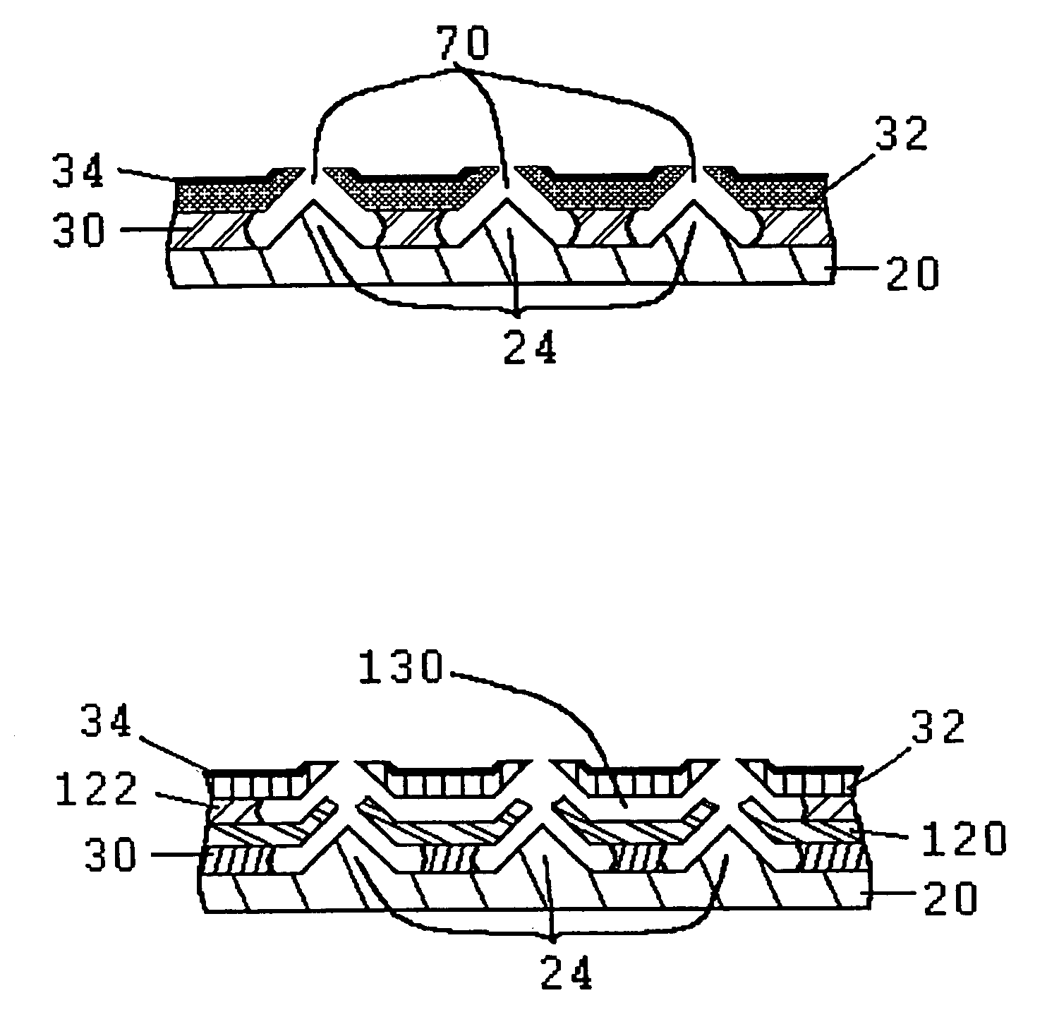
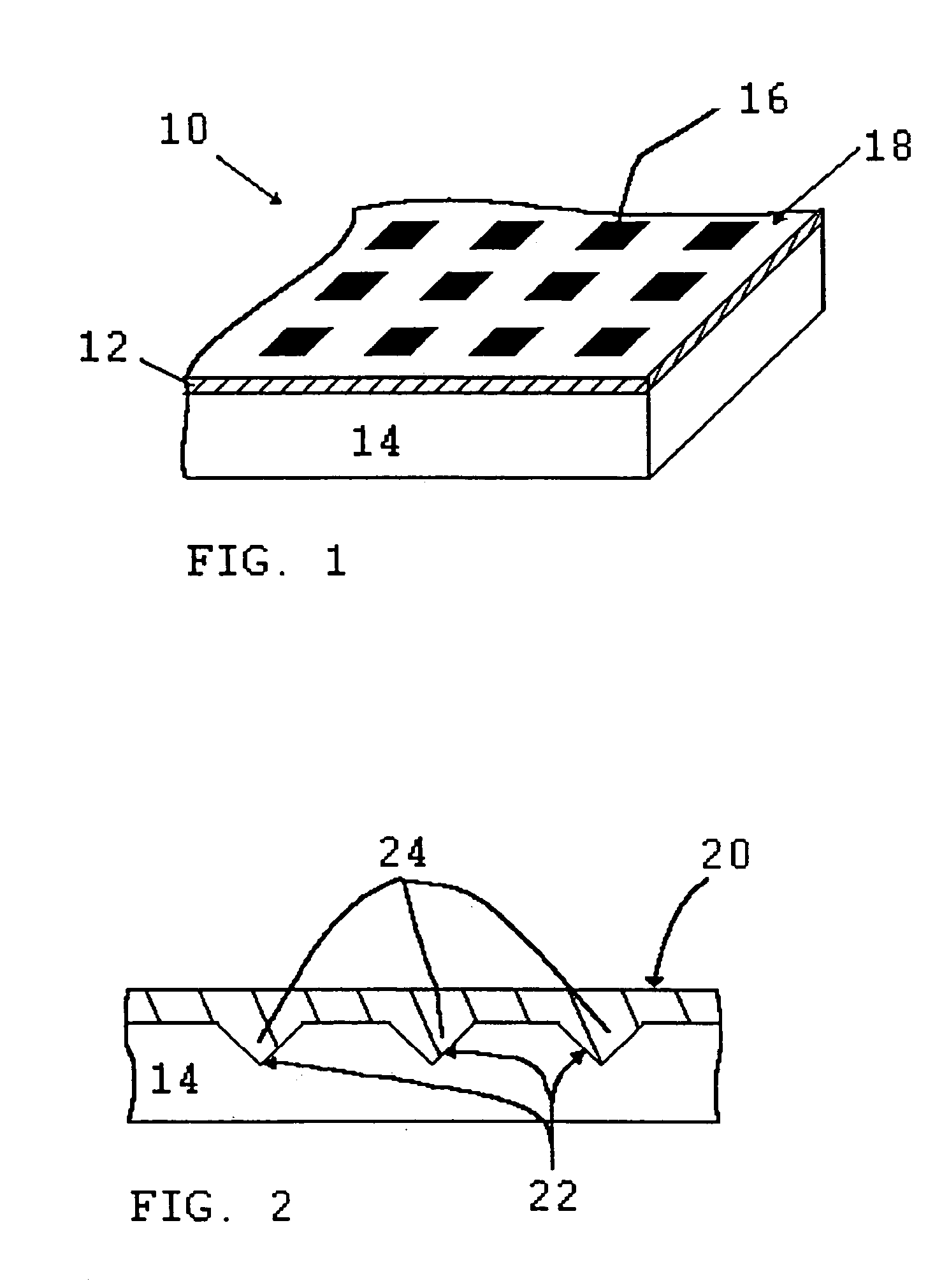
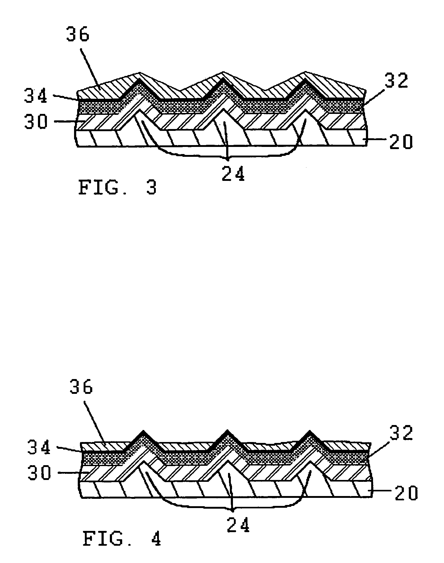
[0024]Reference is now made in detail to the exemplary embodiments of the invention, examples of which are illustrated in the accompanying drawings. Wherever possible, the same reference numbers will be used throughout the drawings to refer to the same or like parts (elements).

[0025]FIG. 1 illustrates a portion of mold 10 that may be produced using common photolithographic techniques. Initially, thin silicon oxide, silicon nitride, or other similar film 12 can be grown on the surface of silicon wafer 14. A template may be created by etching a plurality of openings 16 in the oxide film using conventional photolithographic processes. The openings may be in the shape of squares or circles. The openings may be in the range of about 2 microns per side and can be arranged in groups such that each group forms an array having a selected number of squares, such as group 18. Mold 10 may consist of a plurality of groups. After the openings are defined in the template, the mold can be anisotrop...


PUM


Abstract

A field emission device having emitter tips and a support layer for a gate electrode is provided. Openings in the support layer and the gate layer are sized to provide mechanical support for the gate electrode. Cavities may be formed and mechanically supported by walls between cavities or columns within a cavity. Dielectric layers having openings of different sizes between the emission tips and the gate electrode can decrease leakage current between emitter tips and the gate layer. The emitter tips may comprise a carbon-based material. The device can be formed using processing operations similar to those used in conventional semiconductor device manufacturing.

Description

CROSS-REFERENCE TO RELATED APPLICATIONS[0001]This application is a divisional application of prior U.S. patent application Ser. No. 10 / 035,766, filed on Dec. 26, 2001, now patented U.S. Pat. No. 6,963,160, entitled GATED ELECTRON EMITTER HAVING SUPPORTED GATE,” which is incorporated herein by reference in its entirety for all purposes.BACKGROUND OF THE INVENTION[0002]This invention relates to a device for field emission of electrons. More particularly, apparatus and method for manufacture are provided for a field emitter having a mechanically supported extraction gate. Field emission is a well-known effect in which electrons are induced to leave a cathode material by a strong electric field. The electric field is formed by a grid or gate electrode in proximity to a tip or protrusion of the cathode material. A common problem with field emission devices fabricated with grids or gates in close proximity to a tip of cathode material is that an electrical short-circuit may develop along ...

Claims


Application Information

Patent Timeline
Patent Type & Authority Patents(United States)
IPC IPC(8): H01J9/02H01J1/304H01J3/02
CPCH01J3/022H01J9/025
Inventor SCHUELLER, RANDOLPH D.HONG, LEGAL REPRESENTATIVE, SUSANHONG, DECEASED, CHARLIE C.
Owner ALTERA CORP
Features
  • R&D
  • Intellectual Property
  • Life Sciences
  • Materials
  • Tech Scout
  • Unparalleled Data Quality
  • Higher Quality Content
  • 60% Fewer Hallucinations
Learn More