Method for reducing tungsten film roughness and improving step coverage

a technology of tungsten film and step coverage, which is applied in the field of tungsten film formation, can solve the problems of reducing the sensitivity of pnl tungsten deposition process to variations in the surface conditions of semiconductor substrates, and achieves excellent step coverage and smoothness of pnl-w, and low resistivity of cvd-w. , the effect of high growth ra

Inactive Publication Date: 2006-11-28
NOVELLUS SYSTEMS
View PDF47 Cites 154 Cited by
  • Summary
  • Abstract
  • Description
  • Claims
  • Application Information

AI Technical Summary

Benefits of technology

[0011]In another aspect of the invention, the deposition method forms the tungsten film in a process employing at least three separate deposition operations: (a) depositing a tungsten nucleation layer on the semiconductor substrate; (b) depositing a tungsten bulk layer on the nucleation layer using a chemical vapor deposition (CVD) process; and (c) depositing a tungsten cap layer on the tungsten bulk layer using a pulsed nucleation layer (PNL) deposition technique. Operations (b) and (c) may be repeated multiple times to create a film of the desired thickness which possesses the high growth rate and low resistivity of CVD-W and the excellent step coverage and smoothness of PNL-W.
[0012]In yet another aspect of the invention, the deposition method forms a boron layer on the semiconductor substrate to begin the deposition process. This has been found to reduce the sensitivity of PNL tungsten deposition processes to variations in the surface conditions of the semiconductor substrates. The boron process may be characterized by the following operations: (a) forming a boron layer on the semiconductor substrate; (b) contacting the boron layer with a tungsten-containing gas to thereby reduce the tungsten-containing gas to a tungsten layer on the semiconductor substrate; (c) contacting the semiconductor substrate with a reducing agent to form a layer of reducing agent; and (d) contacting the layer of reducing agent with the tungsten-containing gas to thereby reduce the tungsten-containing gas to another tungsten layer on the semiconductor substrate. Operations (c) and (d) may be repeated for multiple cycles. The boron layer formed in (a) can be deposited at any thickness, as its deposition is not a self-limiting process. But preferably it is maintained as a relatively thin layer. In some embodiments, the reducing agent employed in (c) is a silane or other material that adsorbs on the semiconductor substrate in a self-limiting manner.

Problems solved by technology

This has been found to reduce the sensitivity of PNL tungsten deposition processes to variations in the surface conditions of the semiconductor substrates.

Method used


Image

  • Method for reducing tungsten film roughness and improving step coverage
  • Method for reducing tungsten film roughness and improving step coverage
  • Method for reducing tungsten film roughness and improving step coverage

Examples


Embodiment Construction

[0025]Embodiments of the present invention will be described with reference to the aforementioned figures. These figures are simplified for ease of understanding and description of embodiments of the present invention only. Modifications, adaptations or variations of specific methods and or structures shown and discussed herein may become apparent to those skilled in the art. All such modifications, adaptations or variations that rely upon the teachings of the present invention, and through which these teachings have advanced the art, are considered to be within the spirit and scope of the present invention.

Introduction

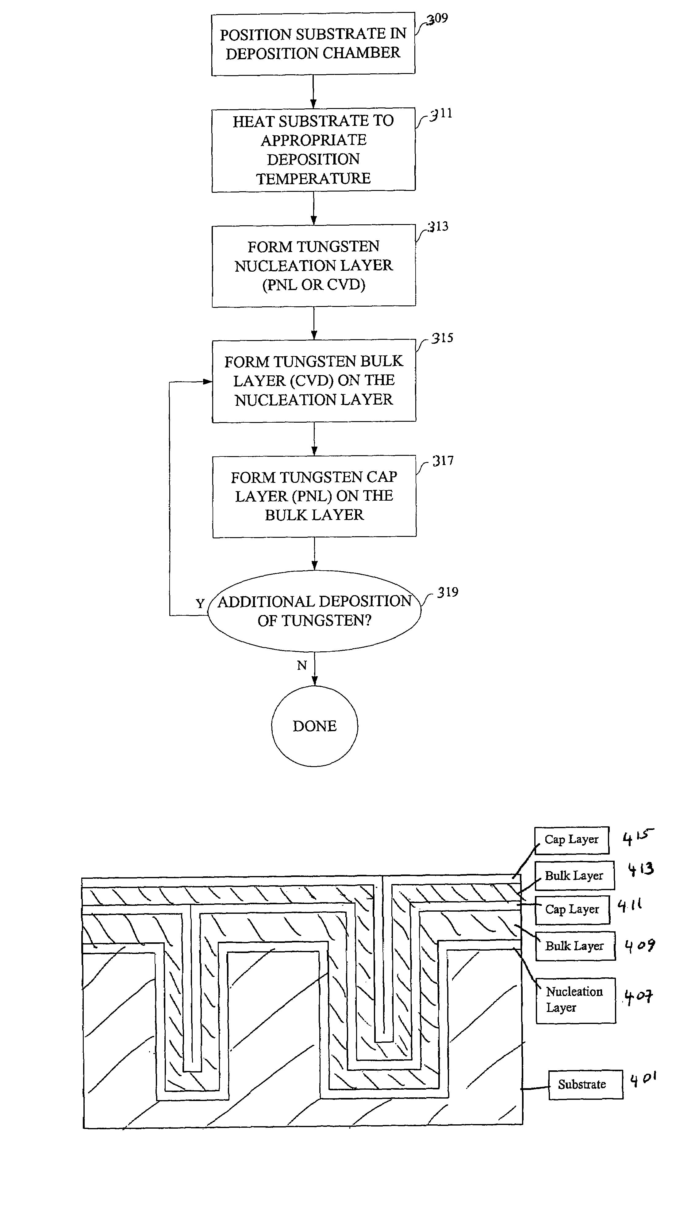
[0026]The present invention provides improved methods of forming a tungsten layer on a semiconductor substrate. It accomplishes this by use of various techniques to control the tungsten deposition process. These include use of nitrogen as a process gas to control nucleation of tungsten, alternating PNL and CVD to form a tungsten layer, and use of a boron sacrificial l...


PUM

PropertyMeasurementUnit
thicknessaaaaaaaaaa
thicknessaaaaaaaaaa
operating pressureaaaaaaaaaa

Abstract

A tungsten nucleation film is formed on a surface of a semiconductor substrate by alternatively providing to that surface, reducing gases and tungsten-containing gases. Each cycle of the method provides for one or more monolayers of the tungsten film. The film is conformal and has improved step coverage, even for a high aspect ratio contact hole.

Description

CROSS-REFERENCE TO RELATED PATENT APPLICATIONS[0001]This application is a continuation in part of U.S. patent application Ser. No. 09 / 975,074 by Lee et al., filed Oct. 9, 2001 now U.S. Pat. No. 6,635,965 and titled “METHOD FOR PRODUCING ULTRA-THIN TUNGSTEN LAYERS WITH IMPROVED STEP COVERAGE,” which in turn claims priority from U.S. Provisional Patent Application No. 60 / 292,917, filed May 22, 2001, by Lee et al., and titled “ULTRA THIN TUNGSTEN LAYER WITH IMPROVED STEP COVERAGE.” Both prior applications are incorporated herein by reference for all purposes.FIELD OF THE INVENTION[0002]The present invention relates to formation of tungsten films on a semiconductor substrate.BACKGROUND OF THE INVENTION[0003]The deposition of tungsten (W) films using chemical vapor deposition (CVD) techniques is an integral part of many semiconductor fabrication processes since it can produce low resistivity electrical connection between (i) adjacent metal layers (vias) and (ii) first metal layer and the...

Claims


Application Information

Patent Timeline
Patent Type & Authority Patents(United States)
IPC IPC(8): H01L21/4763H01L21/44H01L21/283H01L21/285H01L21/768
CPCH01L21/28556H01L21/28562H01L21/76843H01L21/76876H01L21/76877Y10S438/902B65F1/16B65F2210/129
Inventor LEE, SANG-HYEOBLEVY, KARL B.FELLIS, AARON R.WONGSENAKHUM, PANYAGAO, JUWENCOLLINS, JOSHUAASHTIANI, KAIHAN A.SUNG, JUNGHWANCHAN, LANA HIULUI
Owner NOVELLUS SYSTEMS
Why Eureka
Try Eureka