Vertical channel field effect transistors having insulating layers thereon

a field effect transistor and vertical channel technology, applied in the field of vertical channel field effect transistors, can solve the problems of short channel effect, drain induced barrier lowering effect, transistor size reduction, etc., and achieve the effect of preventing the normal operation of the transistor

Active Publication Date: 2006-12-12
HONDA MOTOR CO LTD +1
View PDF6 Cites 54 Cited by
  • Summary
  • Abstract
  • Description
  • Claims
  • Application Information

AI Technical Summary

Benefits of technology

[0018]According to further embodiments of the invention, a transistor can be formed by connecting transistors according to some of the above embodiments, which may improve current driving capacity. For example, the transistor can include a plurality of vertical channels protruding from a substrate having respective source / drain region junctions between the plurality of vertical channels and the substrate, and a plurality of insulating layers extending on respective side walls of the plurality of vertical channels toward the substrate to beyond the respective source / drain region junctions.

Problems solved by technology

Several problems, such as short channel effects and drain induced barrier lowering (DIBL) effects, can occur when transistor size is decreased.
For example, if the channel width of the transistor is reduced to less than 50 nm, distribution of device characteristics may increase, and if the channel width is reduced to less than 30 nm, short channel effects and DIBL effects may occur, thereby hindering normal operation of the transistor.
Thus, the transistor may not be effectively controlled by the gate electrode, which may cause short channel effects.
However, the transistors discussed in the above references are formed on SOI substrate, which can contribute to several problems, such as floating body effect, inferior thermal conductivity, expensive wafer price, and high defect density of the SOI substrate.
The transistor is formed on the buried oxide layer 22 and is separated from the substrate, which can cause low thermal conductivity and floating body effects.

Method used


Image

  • Vertical channel field effect transistors having insulating layers thereon
  • Vertical channel field effect transistors having insulating layers thereon
  • Vertical channel field effect transistors having insulating layers thereon

Examples


Embodiment Construction

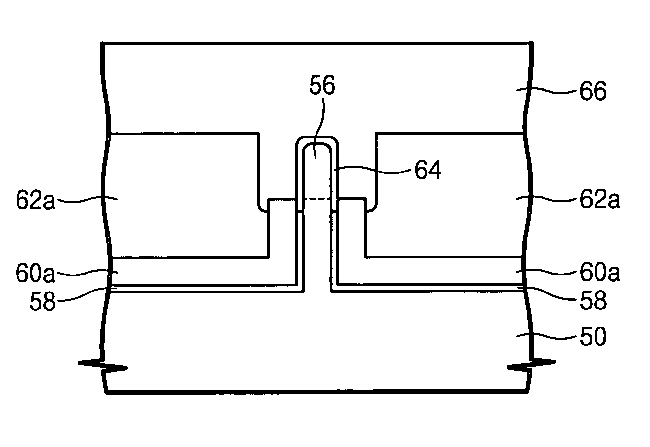
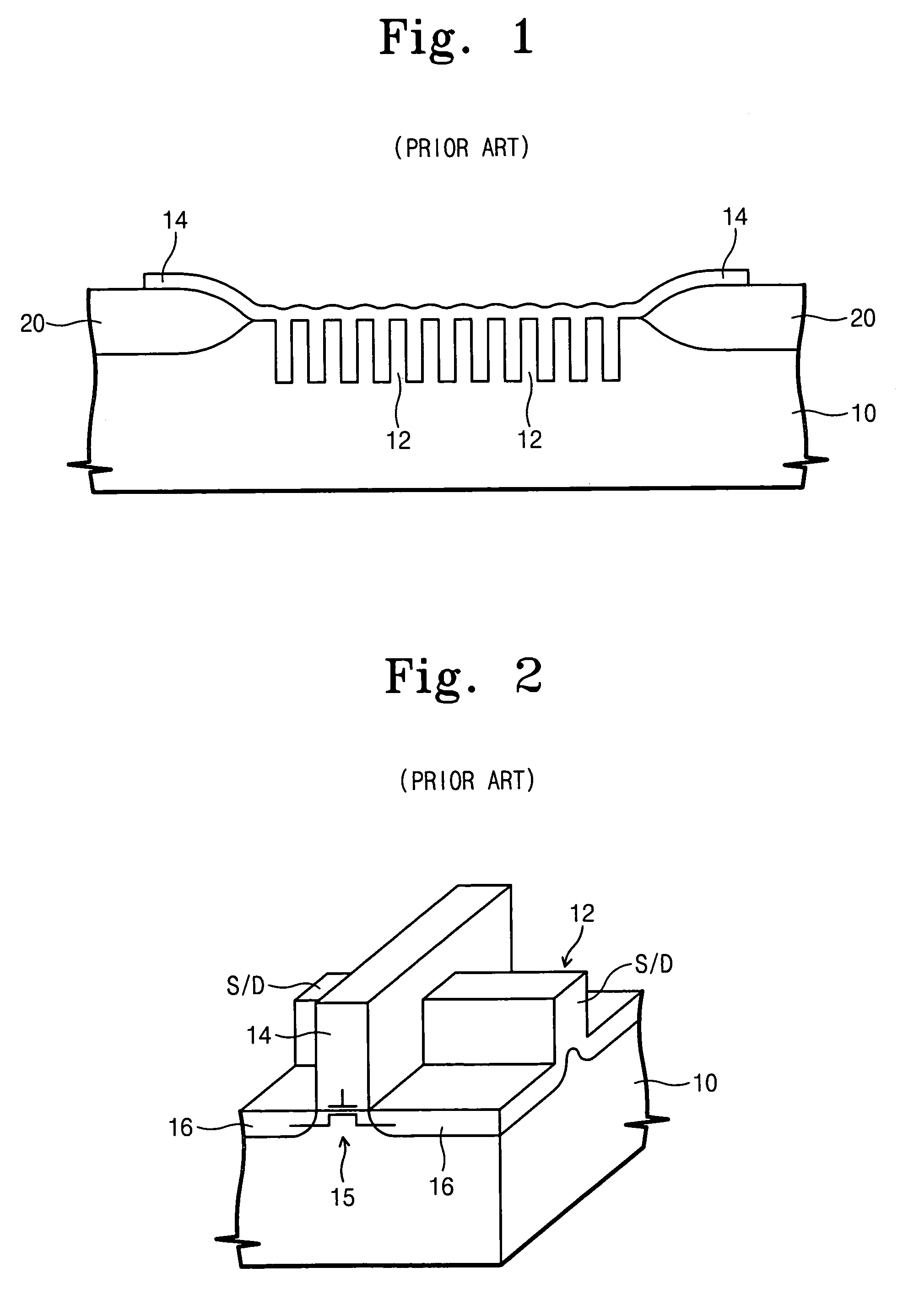
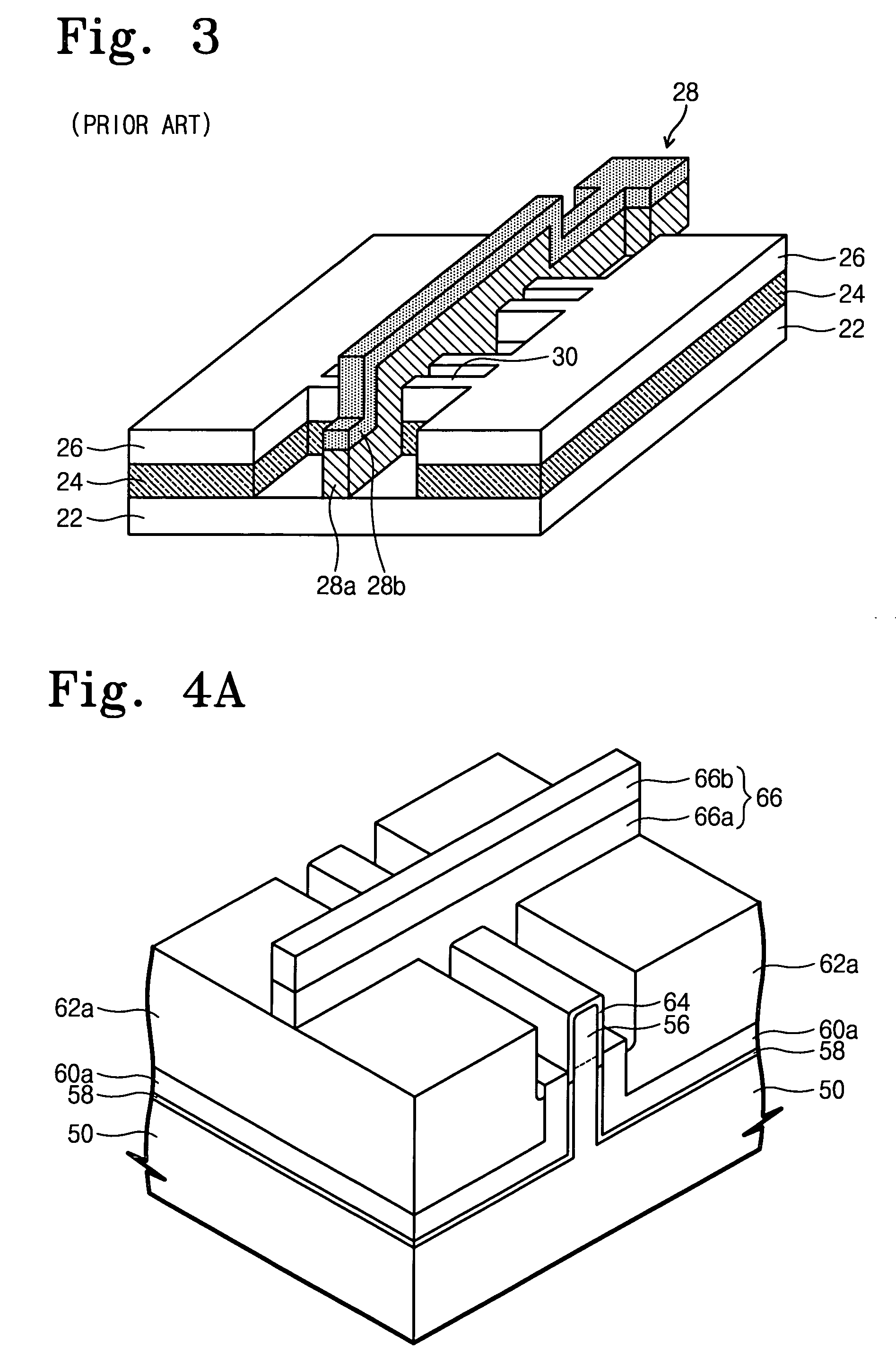
[0035]The present invention will now be described more fully hereinafter with reference to the accompanying drawings, in which embodiments of the invention are shown. This invention may, however, be embodied in different forms, and should not be construed as limited to the embodiments set forth herein. Rather, these embodiments are provided so that this disclosure will be thorough and complete, and will fully convey the scope of the invention to those skilled in the art. In the drawings, the thickness of layers and regions are exaggerated for clarity. It should also be understood that when a layer is referred to as being “on” another layer or substrate, it may be directly on the other layer or substrate, or intervening layers may also be present.

[0036]Furthermore, relative terms, such as “beneath”, are used herein to describe one element's relationship to another as illustrated in the Figures. It will be understood that relative terms are intended to encompass different orientations...


PUM


Abstract

A field effect transistor can include a vertical channel protruding from a substrate including a source / drain region junction between the vertical channel and the substrate, and an insulating layer extending on a side wall of the vertical channel toward the substrate to beyond the source / drain region junction. The transistor can also include a nitride layer extending on the side wall away from the substrate to beyond the insulating layer, a second insulating layer extending on the side wall that is separated from the channel by the nitride layer, and a gate electrode extending on the side wall toward the substrate to beyond the source / drain region junction. Related methods are also disclosed.

Description

RELATED APPLICATION[0001]This application claims priority to Korean Patent Application No. 10-2003-0010402, filed on Feb. 19, 2003, the contents of which are herein incorporated by reference in their entirety.FIELD OF THE INVENTION[0002]The present invention relates to semiconductor devices, and more specifically, to field effect transistors with vertical channels and methods of fabricating the same.BACKGROUND OF THE INVENTION[0003]Several problems, such as short channel effects and drain induced barrier lowering (DIBL) effects, can occur when transistor size is decreased. For example, if the channel width of the transistor is reduced to less than 50 nm, distribution of device characteristics may increase, and if the channel width is reduced to less than 30 nm, short channel effects and DIBL effects may occur, thereby hindering normal operation of the transistor.[0004]In order to overcome these problems, studies on dual gate transistors have increased. Some dual gate transistors can...

Claims


Application Information

Patent Timeline
Patent Type & Authority Patents(United States)
IPC IPC(8): H01L27/01H01L29/78H01L21/336H01L29/786
CPCH01L29/66795H01L29/7851H01L29/7854H01L29/78
Inventor PARK, TAI-SUYOON, EUI-JOONCHUNG, U-INCHOI, SI-YOUNGLEE, JONG-HO
Owner HONDA MOTOR CO LTD
Why Eureka
Try Eureka