Mask defect analysis for both horizontal and vertical processing effects

Inactive Publication Date: 2006-12-12
BELL SEMICON LLC
View PDF10 Cites 11 Cited by
  • Summary
  • Abstract
  • Description
  • Claims
  • Application Information

AI Technical Summary

Benefits of technology

[0011]According to the system and method disclosed herein, the present invention accurately produces input for the process simulator from the image of the physical mask, and analyzes the effects of the defects in the current horizontal layer as well as the vertically adjacent layers in the circuit design.

Problems solved by technology

Unfortunately, errors may occur during the manufacture of the masks that result in mask defects.
A mask defect is any irregularity in the mask that deviates from the mask design.
Using a mask having defects during the photolithography process may produce a circuit pattern on the substrate that fails to accurately represent the intended pattern and that may result in a non-functioning circuit, depending on the severity of the defect.
A mask defect that will not result in any appreciable error in a circuit if the mask is used during fabrication is considered a “unprintable” defect, while a severe defect that may result in a fatal error in the circuit is deemed “printable”, causing the mask to be discarded.
Differences larger than user-defined tolerances are reported as errors.
Although the defect detection systems described above are an improvement over visual inspection systems, current methods for detecting mask defects have disadvantages.
One disadvantage is related to what is used as the input for the process simulation software.
Chang, however, fails to describe how the features of the mask are extracted from the image.
Furthermore, process simulation software typically requires the input data to be in GDSII format, and Chang fails to describe that the digitized data is converted to GDSII format.
If the photograph of the mask is not accurately converted, then the input to the image simulation software will be inaccurate, and so will the resulting simulation.
Another problem with current defect detection systems is that although current detection systems can find mask defects, each defect is analyzed for its effect only on the horizontal processing layer on which the defect is located.
However, as those with ordinary skill in the art will appreciate, mask defects may produce defects that affect adjacent layers in the circuit.
Current defect detection systems fail to test for such “vertical effects.”

Method used


Image

  • Mask defect analysis for both horizontal and vertical processing effects
  • Mask defect analysis for both horizontal and vertical processing effects
  • Mask defect analysis for both horizontal and vertical processing effects

Examples


Embodiment Construction

[0017]The present invention relates to mask defect detection techniques for semiconductor manufacturing. The following description is presented to enable one of ordinary skill in the art to make and use the invention and is provided in the context of a patent application and its requirements. Various modifications to the preferred embodiments and the generic principles and features described herein will be readily apparent to those skilled in the art. Thus, the present invention is not intended to be limited to the embodiments shown but is to be accorded the widest scope consistent with the principles and features described herein.

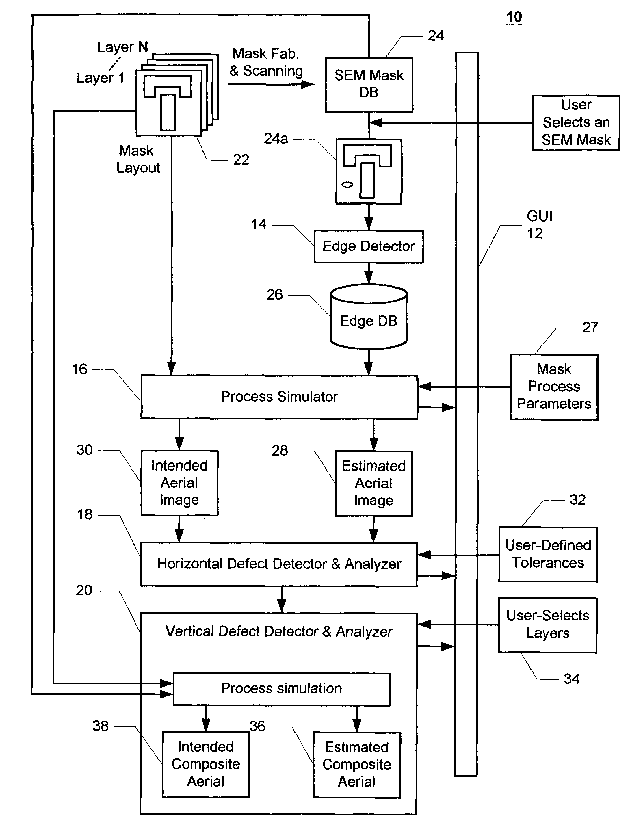
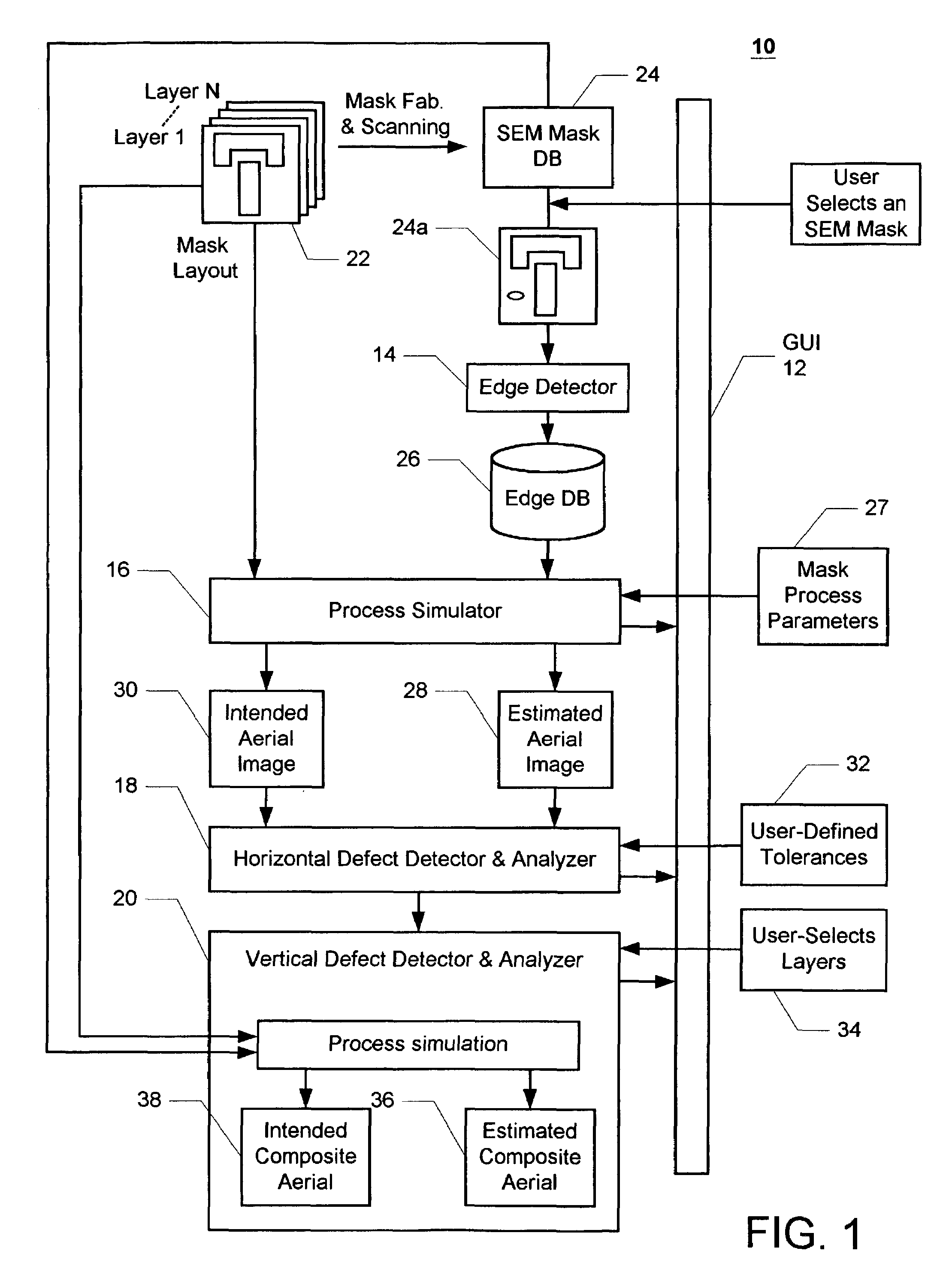
[0018]The present invention provides a mask defect detection and analysis system that accurately produces input for a process simulation application from a digital image of a physical mask. The detection system of the present invention also analyzes the printability of the defects in the horizontal layer as well as the vertical layers in the circuit design...


PUM


Abstract

A method and system for detecting defects in a physical mask used for fabricating a semiconductor device having multiple layers is disclosed, where each layer has a corresponding mask. The method and system include receiving a digital image of the mask, and automatically detecting edges of the mask in the image using pattern recognition. The detected edges, which are stored in a standard format, are imported along with processing parameters into a process simulator that generates an estimated aerial image of the silicon layout that would be produced by a scanner using the mask and the parameters. The estimated aerial image is then compared to an intended aerial image of the same layer, and any differences found that are greater than predefined tolerances are determined to horizontal defects. In addition, effects that the horizontal defects may have on adjacent layers are analyzed to discover vertical defects.

Description

FIELD OF THE INVENTION[0001]The present invention relates to detecting mask defects in semiconductor masking photolithographic processes, and more particular to analyzing the effects of any detected defects via aerial / latent image simulations using a photograph of the mask as input.BACKGROUND OF THE INVENTION[0002]An integrated circuit is fabricated by translating a circuit design or layout to a semiconductor substrate. In optical lithography, the layout is first transferred onto a physical template, which is in turn, used to optically project the layout onto a silicon wafer. In transferring the layout to a physical template, a mask is generally created for each layer of the integrated circuit design.[0003]The patterned photomask includes transparent and opaque areas for selectively exposing regions of the photoresist-coated wafer to an energy source. To fabricate a particular layer of the design, the corresponding mask is placed over the wafer and light is shone through the mask fr...

Claims


Application Information

Patent Timeline
IPC IPC(8): G06K9/00G03F1/84G06T7/00G06V10/46
CPCG03F1/84G06K9/48G06K9/6206G06T7/001G06T2207/30148G06V10/46G06V10/754
Inventor FILSETH, PAULCALLAN, NEALTARAVADE, KUNALGARZA, MARIO
Owner BELL SEMICON LLC
Why Eureka
Try Eureka