Apparatus and method for depositing and planarizing thin films of semiconductor wafers

a technology of semiconductor wafers and apparatuses, applied in the field of semiconductor wafer deposition and planarization, can solve the problems of limiting the efficiency of surface activation steps, limiting the productivity of plating operations, and significant negative impact on wafer throughput and increasing processing costs, so as to reduce the active area of plating, improve chemical exchange, and reduce the total plating current

Inactive Publication Date: 2006-12-26
LAM RES CORP
View PDF93 Cites 34 Cited by
  • Summary
  • Abstract
  • Description
  • Claims
  • Application Information

AI Technical Summary

Benefits of technology

[0017]The advantages of the present invention are numerous, most notably; the embodiments enable localized plating thereby reducing the active area of plating and improving chemical exchange. Localized metallic plating reduces the total plating current that must be distributed over the seed layer, thereby significantly reducing the resistive seed layer effect and improving deposit uniformity. In-situ film thickness control and planarization produce increased productivity by reducing the number of wafer transfers during processing, and consolidating several applications on one piece of equipment. Other aspects and advantages of the present invention will become apparent from the following detailed description, taken in conjunction with the accompanying drawings, illustrating by way of example the principles of the present invention.

Problems solved by technology

Due to electrolyte dilution concerns and increased hardware design complexity, DI water rinsing is typically not done within the plating chamber.
Today, approximately fifty percent of the wet processing stations on a wafer plating tool are dedicated to plating, having a significant negative impact on wafer throughput and increasing processing cost.
The additional time, to rinse after surface activation and to transport the wafer to the plating module, significantly limits the effectiveness of the surface activation step.
In some cases, cleaning of the contacts requires additional steps further limiting the productivity of the plating operation.
Another challenge in copper electroplating is a bipolar effect, observed when the contact resistance is very high.
Unfortunately, seals are not perfect and contacts become contaminated and current distribution in the contacts along the wafer periphery results in non-uniform plating.
Additional adverse physical challenges occur when applying the contacts to the surface of the wafer.
Application of such force can, in some cases cause defects on the wafer due to mechanical stresses on certain materials, such as porous low-k dielectric films.
Since the role of the seed layer is to distribute the plating current over the entire wafer during electroplating, a thinner more resistive seed layer introduces a significant challenge in chambers designed for uniform plating near contacts on the wafer periphery.

Method used


Image

  • Apparatus and method for depositing and planarizing thin films of semiconductor wafers
  • Apparatus and method for depositing and planarizing thin films of semiconductor wafers
  • Apparatus and method for depositing and planarizing thin films of semiconductor wafers

Examples


Embodiment Construction

[0029]An invention, for methods and apparatuses for electroplating surfaces of a substrate, is disclosed. In the following description, numerous specific details are set forth in order to provide a thorough understanding of the present invention. It will be understood, however, by one of ordinary skill in the art, that the present invention may be practiced without some or all of these specific details. In other instances, well known process operations have not been described in detail in order not to unnecessarily obscure the present invention.

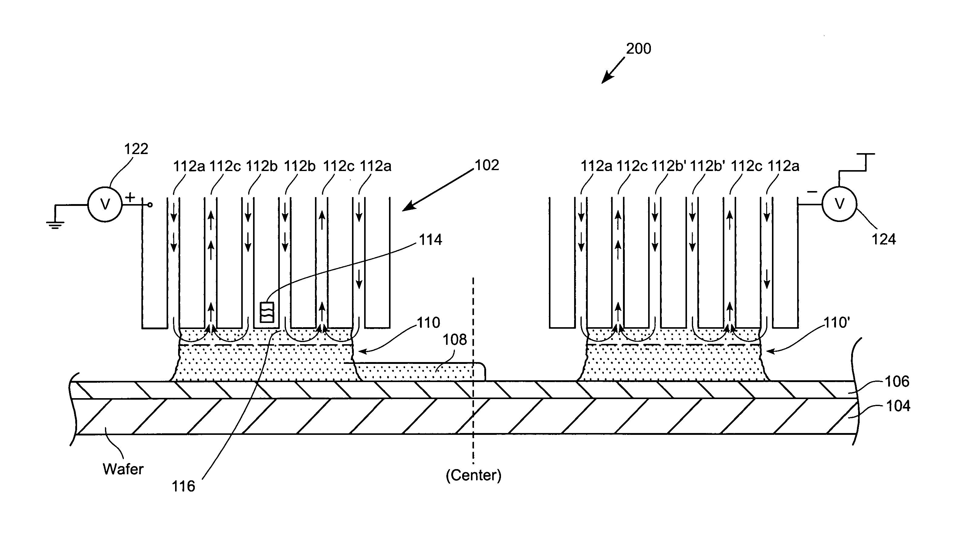
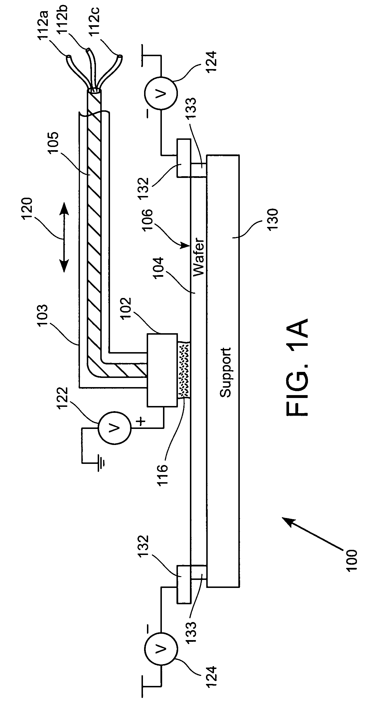
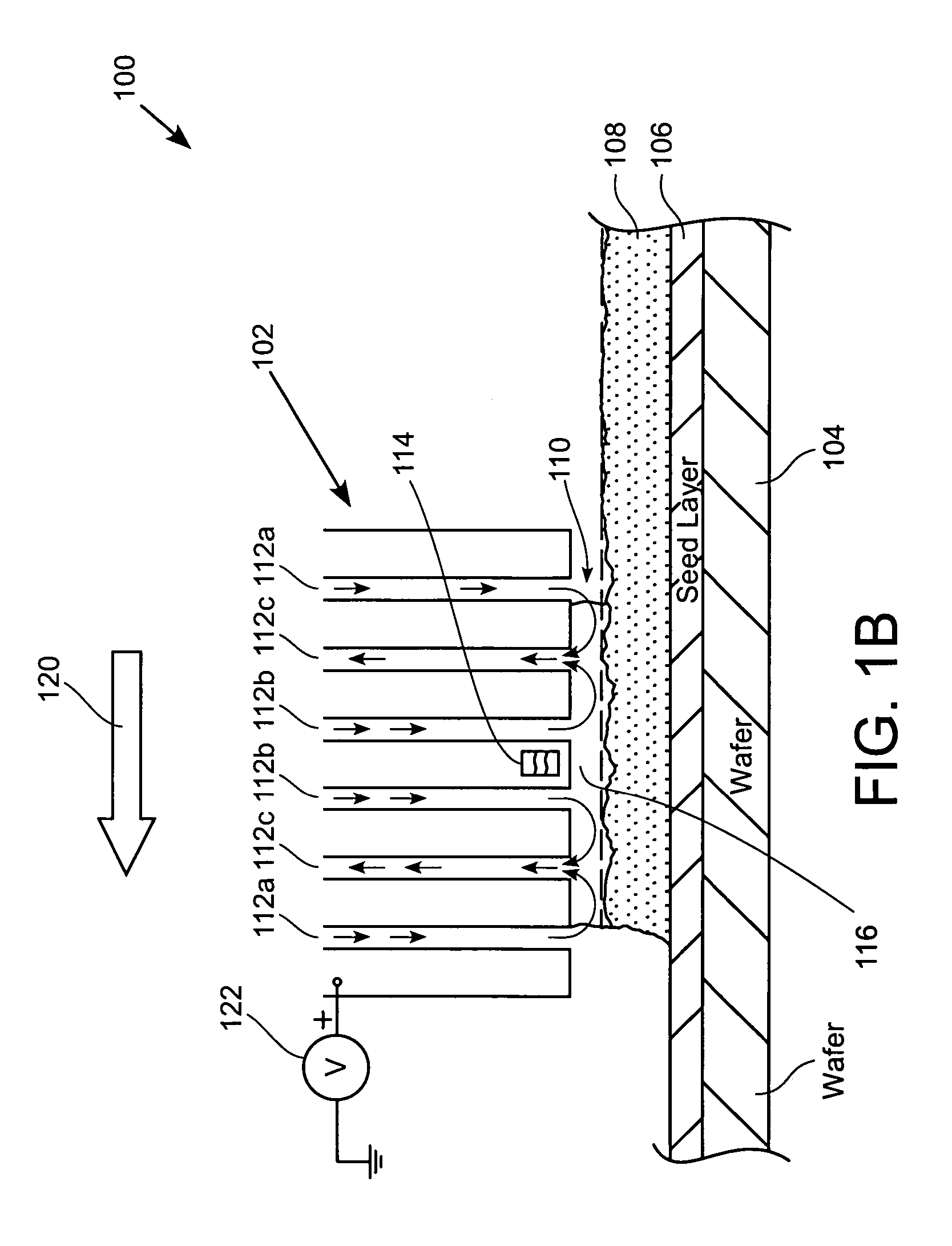
[0030]FIG. 1A is a drawing of an exemplary electroplating apparatus 100 in accordance with one embodiment of the present invention. A wafer 104 with a seed layer 106 is placed on a support 130. A negative bias power supply 124 charges the wafer 104 to function as a cathode by way of electrical contact 132. Electrical contact 132 may be established in the form of a single ring surrounding the wafer 104, an individual mechanical contact, or a p...


PUM

PropertyMeasurementUnit
thicknessaaaaaaaaaa
thicknessaaaaaaaaaa
thicknessaaaaaaaaaa

Abstract

An electroplating apparatus for depositing a metallic layer on a surface of a wafer is provided. In one example, a proximity head capable of being electrically charged as an anode is placed in close proximity to the surface of the wafer. A plating fluid is provided between the wafer and the proximity head to create localized metallic plating.

Description

CROSS REFERENCE TO RELATED APPLICATION[0001]This application is a continuation-in-part and claims 35 U.S.C. § 120 priority from U.S. patent application Ser. No. 10 / 330,843 filed on Dec. 24, 2002 and entitled “Meniscus, Vacuum, IPA Vapor, Drying Manifold,” which is a continuation-in-part of co-pending U.S. patent application Ser. No. 10 / 261,839 filed on Sep. 30, 2002 and entitled “Method and Apparatus for Drying Semiconductor Wafer Surfaces Using a Plurality of Inlets and Outlets Held in Close Proximity to the Wafer Surfaces,” both of which are incorporated herein by reference in their entirety.BACKGROUND OF THE INVENTION[0002]1.Field of the Invention[0003]The present invention relates to semiconductor wafer deposition and planarization and, more particularly, to apparatuses and techniques for more effectively depositing thin films using localized deposition and for enabling localized planarization.[0004]2.Description of the Related Art[0005]Electroplating is a well-established depos...

Claims


Application Information

Patent Timeline
Patent Type & Authority Patents(United States)
IPC IPC(8): C25D17/02C25D5/04C25D5/06C25D7/12C25D5/02C25D5/22H01L21/00H01L21/288
CPCC25D5/026C25D5/22C25D17/10H01L21/2885H01L21/67028H01L21/67034H01L21/67051C25D7/123C25D17/001H01L21/67017
Inventor RAVKIN, MIKEBOYD, JOHNDORDI, YEZDI N.REDEKER, FRED C.DE LARIOS, JOHN M.
Owner LAM RES CORP
Why Eureka
Try Eureka