Apparatus for Plating Semiconductor Wafers

a technology of semiconductor wafers and apparatuses, which is applied in the direction of manufacturing tools, electric circuits, electric circuits, etc., can solve the problems of limiting the productivity of plating operations, affecting the processing efficiency of semiconductor wafers, and affecting the throughput of semiconductor wafers, so as to reduce the active area of plating, improve chemical exchange, and reduce the total plating current

Active Publication Date: 2009-12-31
LAM RES CORP
View PDF6 Cites 3 Cited by
  • Summary
  • Abstract
  • Description
  • Claims
  • Application Information

AI Technical Summary

Benefits of technology

[0017]The advantages of the present invention are numerous, most notably; the embodiments enable localized plating, thus reducing the active area of plating and improving chemical exchange. Localized metallic plating reduces the total plating current that must be distributed over a barrier or seed layer, thereby significantly reducing the resistive layer effect and improving deposit uniformity. Constant monitoring and control of voltage applied by the anode provides uniform current density across the surface of a wafer undergoing plating operations. Concurrent pre-treatment, plating, rinsing and drying techniques consolidate processing producing a more efficient methodology. For example, by having pre-clean and plating processes in an adjacent configuration, local processing ambient conditions can be maintained relatively oxygen-free. Inert gas curtains can be used to prevent re-oxidation of the activated surface region formed between the pre-clean and plating process steps. Other aspects and advantages of the present invention will become apparent from the following detailed description, taken in conjunction with the accompanying drawings, illustrating by way of example the principles of the present invention.

Problems solved by technology

Due to electrolyte dilution concerns and increased hardware design complexity, DI water rinsing is typically not done within the plating chamber.
Today, approximately fifty percent of the wet processing stations on wafer plating tools are dedicated to plating, having a significant negative impact on wafer throughput and increasing processing cost.
The effectiveness of the surface activation operation is limited by additional time taken to rinse a wafer after surface activation and to transport the wafer to the plating module.
In some cases, cleaning of the contacts requires additional processes that further limit the productivity of plating operations.
Bipolar effects are another challenge in copper electroplating, and are observed when contact resistance is very high.
Bipolar effects are avoided when dry contacts are used, however dry contact methods require complicated seal design and are prone to reliability problems.
Since the role of the seed layer is to distribute the plating current over the entire wafer during electroplating, a thinner more resistive seed layer introduces a significant challenge in chambers designed for uniform plating near contacts on the wafer periphery.

Method used


Image

  • Apparatus for Plating Semiconductor Wafers
  • Apparatus for Plating Semiconductor Wafers
  • Apparatus for Plating Semiconductor Wafers

Examples


Embodiment Construction

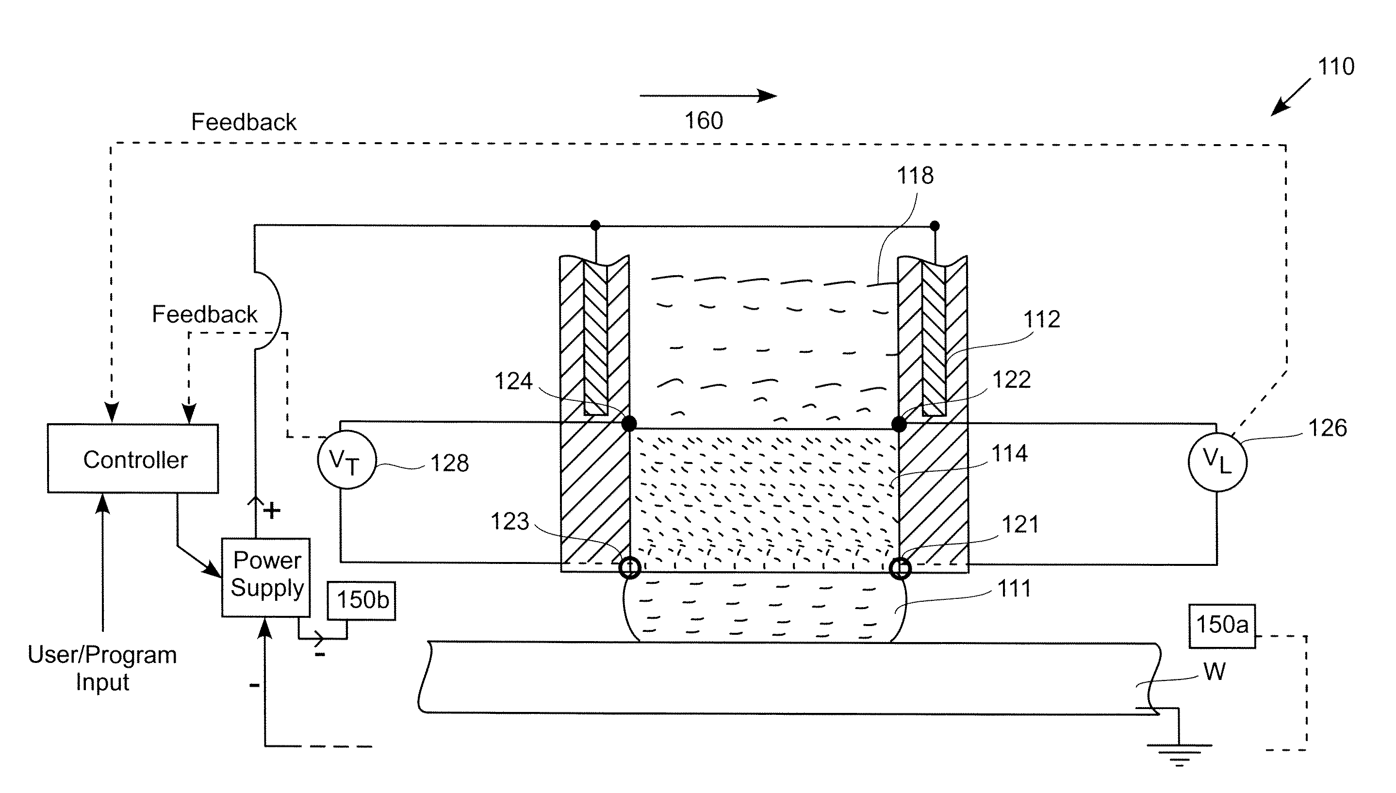
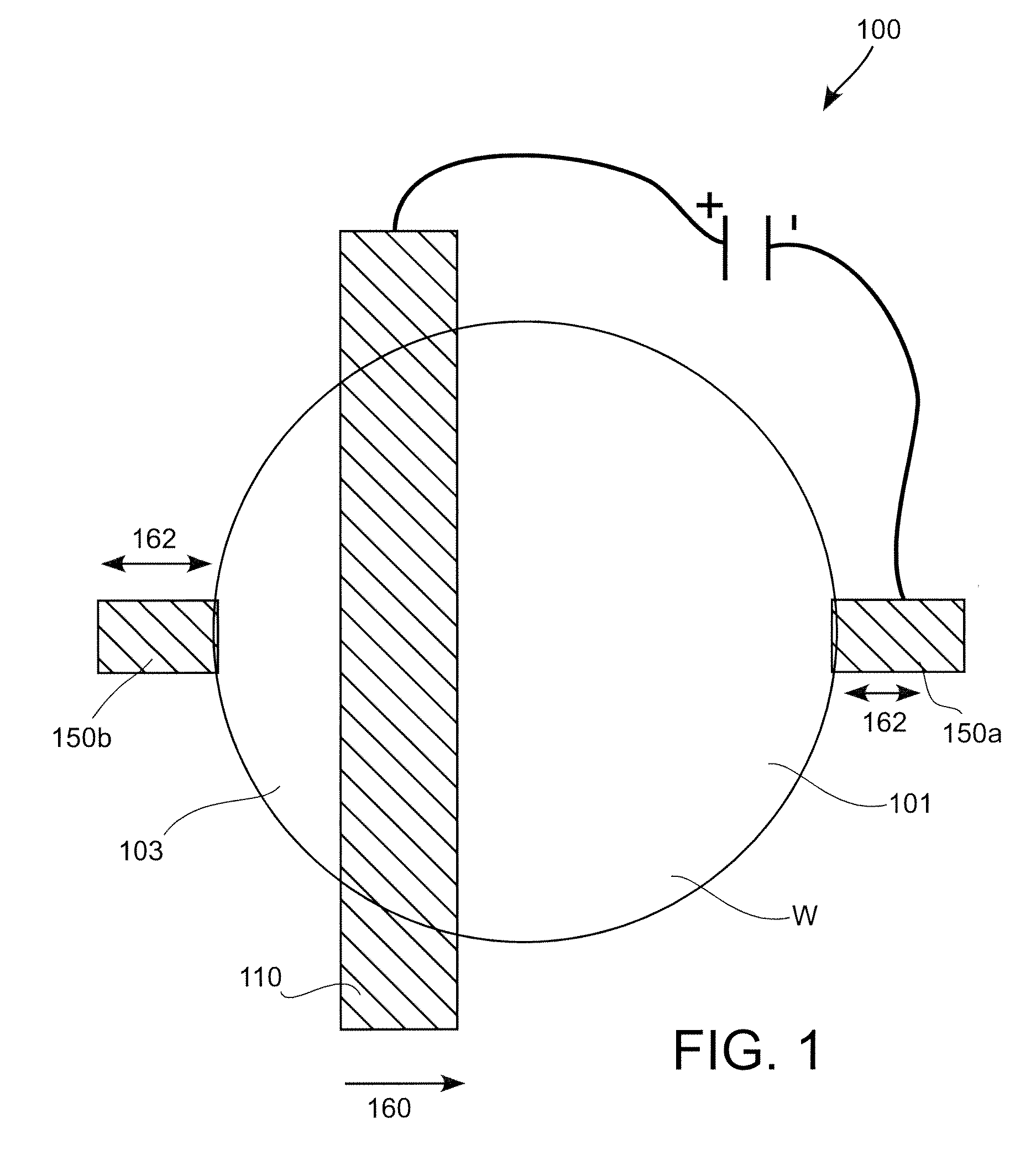
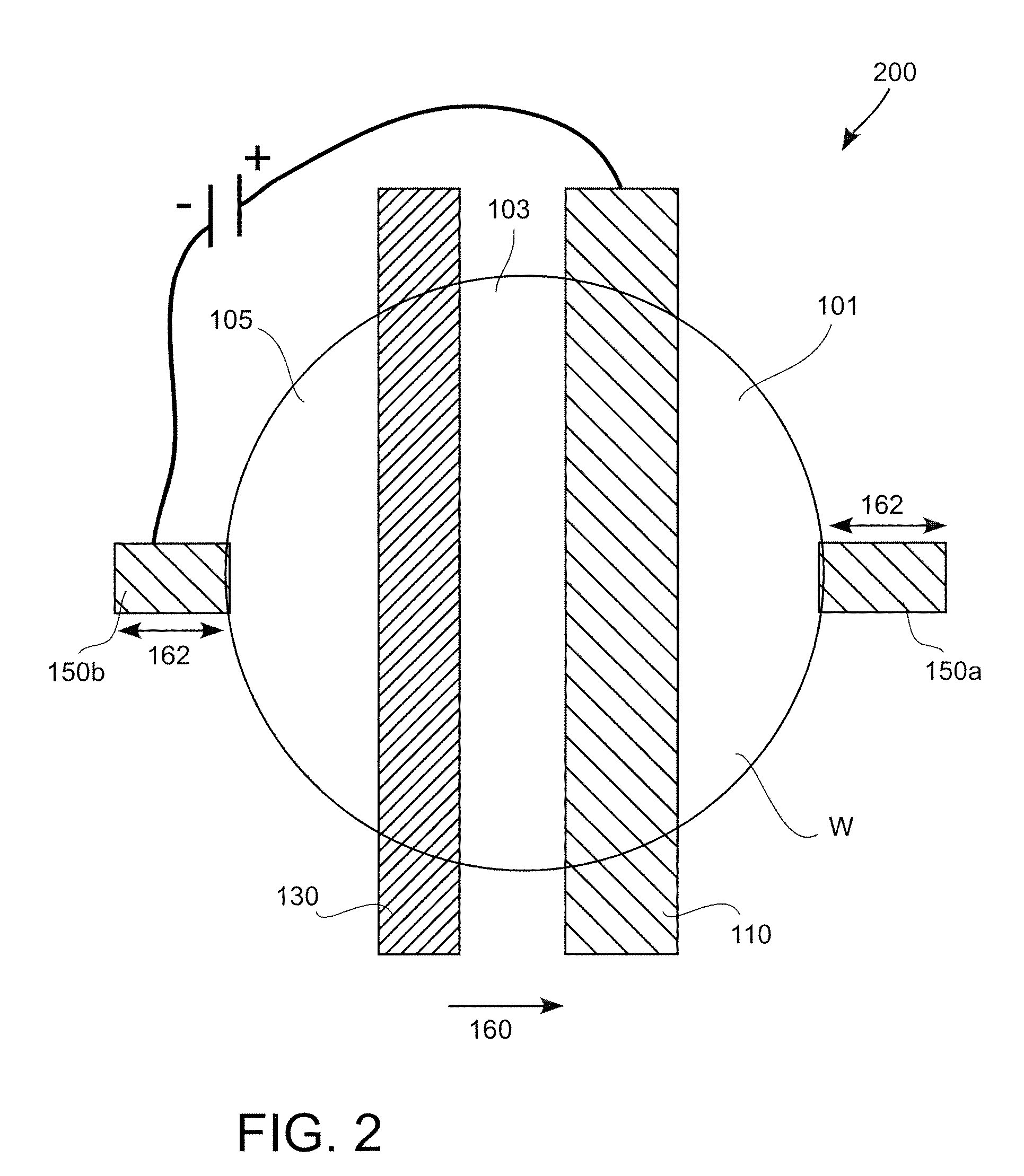
[0035]An invention, for methods and apparatuses for electroplating surfaces of a wafer, is disclosed. The present invention generally provides electrical contact in dry regions of a semiconductor wafer while producing uniform electroplating on barrier. Integrated rinsing processes are provided in an effort to reduce exposure time to electrolyte and consolidate processing. To ensure layer uniformity, the present invention implements single point dry electrical contact with a wafer while maintaining constant voltage, thereby evenly distributing current density across a wafer.

[0036]The following description provides further advancements in the field of plating techniques in the semiconductor arts. In the following description, numerous specific details are set forth in order to provide a thorough understanding of the present invention. It will be understood, however, by one of ordinary skill in the art, that the present invention may be practiced without some or all of these specific d...


PUM

PropertyMeasurementUnit
thicknessaaaaaaaaaa
thicknessaaaaaaaaaa
thicknessaaaaaaaaaa

Abstract

An electroplating apparatus for electroplating a surface of a wafer is provided. The wafer is capable of being electrically charged as a cathode. The electroplating apparatus includes a plating head capable of being positioned either over or under the surface of a wafer and capable of being electrically charged as an anode. The plating head is capable of enabling metallic plating between the surface of the wafer and the plating head when the wafer and plating head are charged. The plating head further comprises a voltage sensor pair capable of sensing a voltage present between the plating head and the surface of the wafer, and a controller capable of receiving data from the voltage sensor pair. The data received from the voltage sensor pair is used by the controller to maintain a substantially constant voltage to be applied by the anode when the plating head is placed in positions over the surface of the wafer. A method of electroplating a wafer is also provided.

Description

CLAIM OF PRIORITY[0001]This application is a continuation of prior application Ser. No. 10 / 882,712, filed on Jun. 30, 2004, from which priority under 35 U.S.C. § 120 is claimed. The disclosure of this application is incorporated herein by reference.CROSS REFERENCE TO RELATED APPLICATION[0002]This application is related to U.S. patent application Ser. No. 10 / 330,843 filed on Dec. 24, 2002 and entitled “Meniscus, Vacuum, IPA Vapor, Drying Manifold,” U.S. patent application Ser. No. 10 / 261,839 filed on Sep. 30, 2002 and entitled “Method and Apparatus for Drying Semiconductor Wafer Surfaces Using a Plurality of Inlets and Outlets Held in Close Proximity to the Wafer Surfaces,” U.S. patent application Ser. No. 10 / 186,472, entitled “Integration of Sensor Based Metrology into Semiconductor Processing Tools”, and filed on Jun. 28, 2002, U.S. patent application Ser. No. 10 / 607,611 filed on Jun. 27, 2003 and entitled “Apparatus and Method for Depositing and Planarizing Thin Films of Semicondu...

Claims


Application Information

Patent Timeline
Patent Type & Authority Applications(United States)
IPC IPC(8): C25D21/12
CPCC25D5/06C25D21/12H01L21/2885C25D17/001C25D17/14C25D7/123
Inventor DORDI, YEZDI N.REDEKER, FRED C.BOYD, JOHN M.MARASCHIN, ROBERTWOODS, CARL
Owner LAM RES CORP
Why Eureka
Try Eureka