

Optical recording/reproducing method and optical recording medium
- Summary
- Abstract
- Description
- Claims
- Application Information
AI Technical Summary
Benefits of technology
Problems solved by technology
Method used
Image

Examples
examples and compared examples
[0093]Now the present invention will be explained more specifically along with some examples, but the invention is not limited to those examples.
[Preparation of the Optical Recording Medium]
Example(s) 1–3
[0094]Optical recording media were fabricated via the following steps.
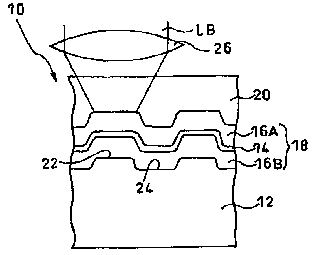
[0095]First, a polycarbonate substrate of which thickness was 1.1 mm and diameter was 120 mm was set in a sputtering apparatus. On the light reflection layer (only in example 2) of this polycarbonate substrate, the second dielectric layer made of a mixture of ZnS and SiO2, the assisting material layer made of Sn and the first dielectric layer (only in examples 1 and 2) made of a mixture of ZnS and SiO2 were formed one after another by the sputtering method.
[0096]Next, on the first dielectric layer, an acrylic ultraviolet-curable resin was coated by the spin coating method and the light transmission layer (thickness: 100 μm) was formed by ultraviolet irradiation thereon.
[0097]The molar ratio between ZnS and SiO2 in...
examples 15
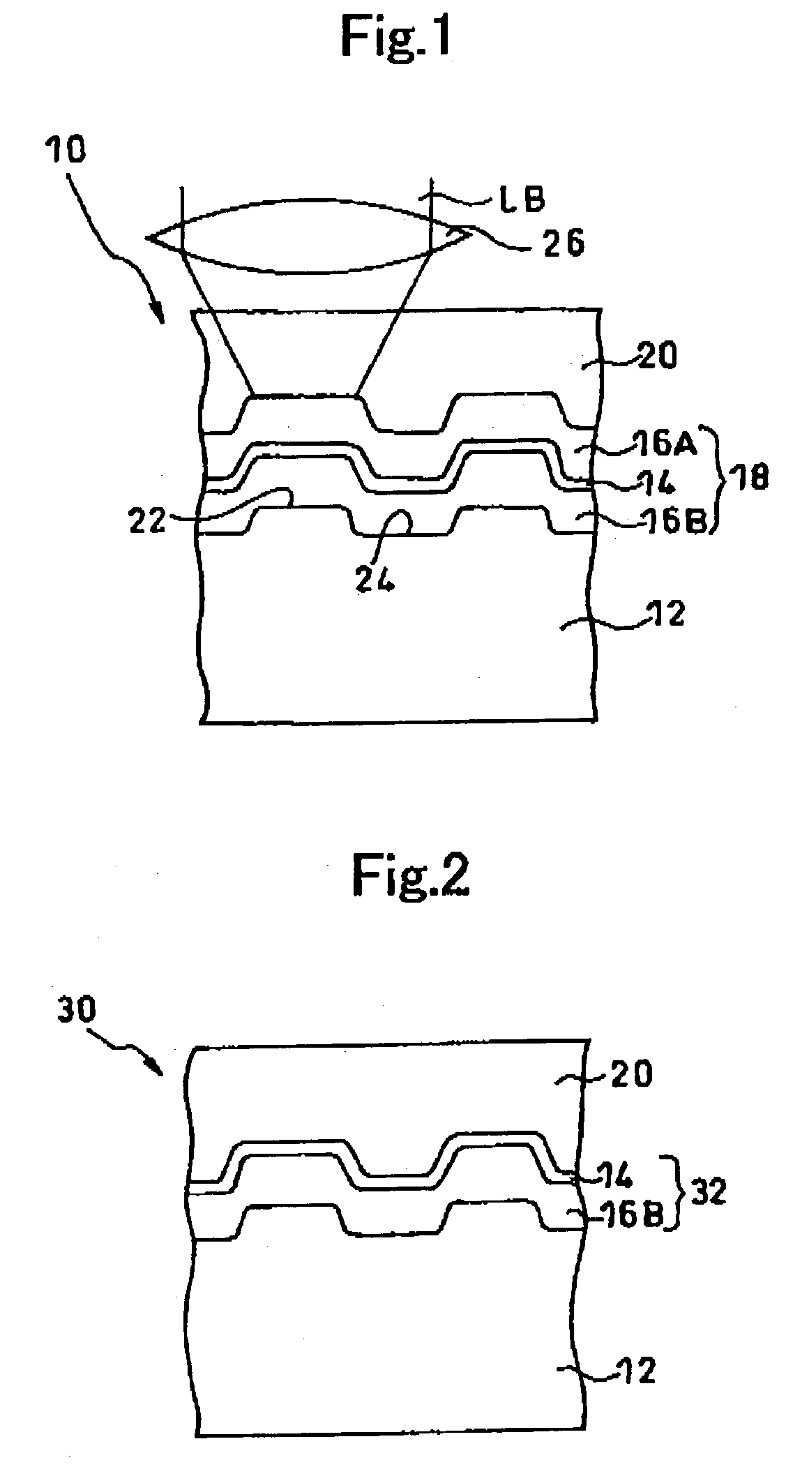
[0100]The optical recording medium with a single-layered recording layer was fabricated without forming any dielectric layer. The recording layer was made of a mixture of Sn and a dielectric material of ZnS:SiO2=80:20.
Example(s) 16, 17
[0101]The optical recording medium was fabricated in the same manner as the example 15 except that Sn employed in the example 15 was replaced by Ag or Ti.
compared example 4
[0102]The optical recording medium was fabricated in the same manner as the example 15 except that ZnS—SiO2 in the example 15 was omitted.
Example(s) 18–21
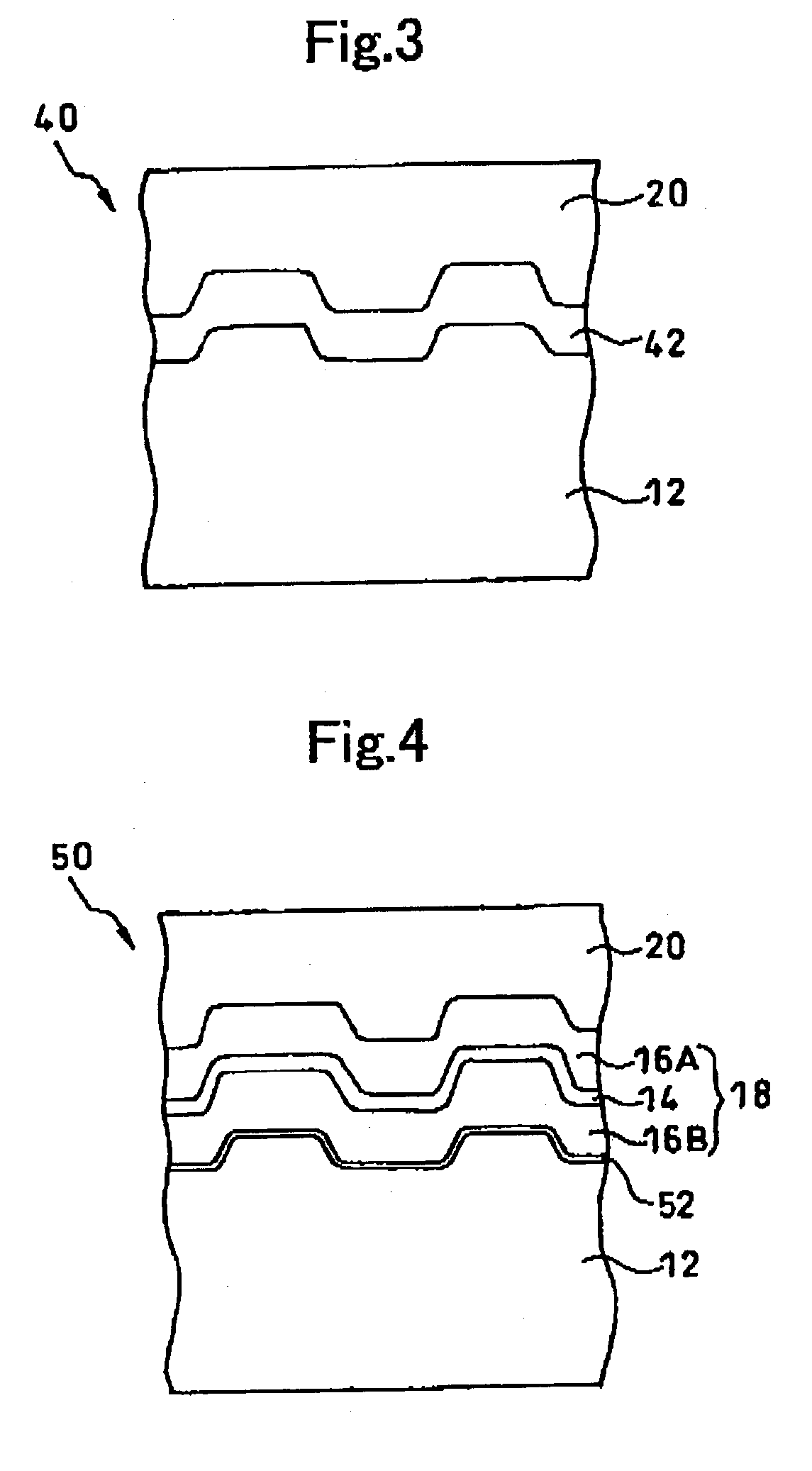
[0103]The optical recording medium was fabricated by changing the material for the dielectric layer and forming the state-change assisting layer made of Sn.
Example(s) 22–30
[0104]The optical recording medium with a recording layer of a single-layer structure was fabricated without forming any dielectric layer. The recording layer was made of a mixture of ZnS—SiO2 (ZnS:SiO2=80:20) and a metal or semi-metal of Mg, Nb, Bi, Mg, Au, Al, Au, Cu, Ta, or Si.
Example(s) 31–52
[0105]The optical recording media were fabricated by replacing ZnS—SiO2 (ZnS:SiO2=80:20) employed in the examples 22–30 to other materials. Mg (examples 31–35), Ti (examples 36–43), Sn (examples 44, 45), Nb (examples 46–48), or Al (examples 49–52) was mixed in the optical recording medium.
Example(s) 53–55
[0106]The optical recording medium with a recording layer of a singl...
PUM
 Abstract
Description
Claims
Application Information