Absorbance detection system for lab-on-a-chip

Inactive Publication Date: 2007-01-02
POSTECH ACAD IND FOUND
View PDF1 Cites 24 Cited by
  • Summary
  • Abstract
  • Description
  • Claims
  • Application Information

AI Technical Summary

Benefits of technology

[0019]To solve the above problems, it is an object of the present invention to provide a high-efficiency, high-sensitivity absorbance detection system in a lab-on-a-chip in which detection cells with long optical pathlen

Problems solved by technology

The electrochemical method also has a high detection sensitivity but its application is limited to specific compounds.
Sensitivity of the absorption detection is usually poor in CE.
Although the lab-on-a-chip-based analytical systems described above are advantageous in that the consumption of sample and reagents is reduced and the analysis can be performed within a short period of time, they cannot be applied

Method used


Image

  • Absorbance detection system for lab-on-a-chip
  • Absorbance detection system for lab-on-a-chip
  • Absorbance detection system for lab-on-a-chip

Examples


Example

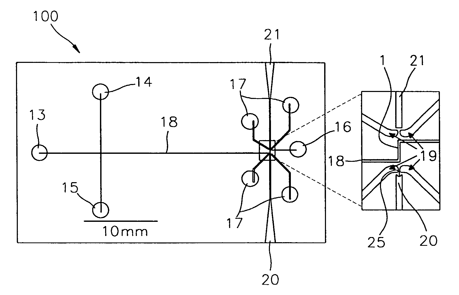
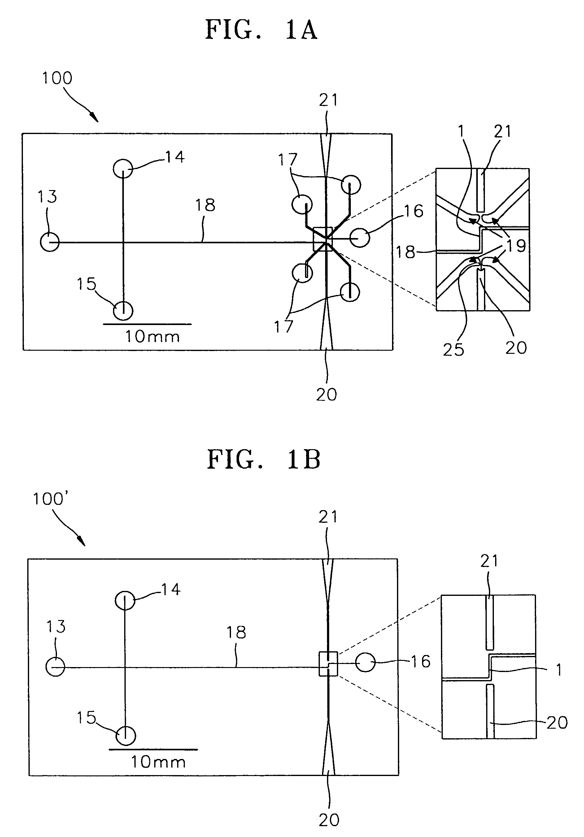
[0038]Preferred embodiments of an absorbance detection system for a lab-on-a-chip according to the present invention will be described in detail with reference to the appended drawings. Description of the prior art or the unnecessary structure of the present invention that makes the subject matter obscure will be omitted. The terms used in the following description are defined on the basis of functions, and thus it will be appreciated by those skilled in the art that the terms may be changed appropriately based on users' or operators' intentions and practices without departing from the meaning intended in the following description.

[0039]FIGS. 1A and 1B show preferred embodiments of an absorbance detection system in a “lab-on-a-chip” according to the present invention. In particular, FIG. 1A shows a high-performance absorbance detection system 100 built in a lab-on-a-chip having a collimator, and FIG. 1B shows an absorbance detection system 100′ built in a lab-on-a-chip that does not...


PUM

PropertyMeasurementUnit
Lengthaaaaaaaaaa
Lengthaaaaaaaaaa
Efficiencyaaaaaaaaaa

Abstract

A high-efficiency, high-sensitivity absorbance detection system in a lab-on-a-chip is provided. The absorbance detection system includes detection cells having an optical pathlength ten times and/or much longer than the width of a separation channel to improve detection sensitivity, lens structures for collimating light in the detection cells, and slit structures for preventing scattered light from entering detectors. The detection cells, the lens structures, and the slit structures of the absorbance detection system are fabricated and integrated in a lab-on-a-chip. The absorbance detection system exhibits excellent absorption efficiency, detection limit, and linearity, compared to existing absorbance detection systems, and can be applied for the detection of a variety of samples. The absorbance detection system does not need labeling of the samples which saves time and costs. The absorbance detection system can be used effectively in detecting trace compounds with a high sensitivity. The absorbance detection system in a lab-on-a-chip can be used with wider applications to a variety of samples in diverse research fields, such as the drug screening field dealing with simultaneous synthesis and identification of a number of compounds based on combinatorial chemistry, the life sciences field handling trace bioactive materials such as enzymes, proteins, and amino acids, and the environmental research field which needs rapid field monitoring of contaminants.

Description

BACKGROUND OF THE INVENTION[0001]1. Field of the Invention[0002]The present invention relates to an absorbance detection system in a lab-on-a-chip, and more particularly, to a high-efficiency, high-sensitivity absorbance detection system in which detection cells with long optical path lengths for higher detection sensitivity, micro-lenses for collimating light into the detection cells, and slits for preventing scattered light from entering detectors are fabricated and integrated in a lab-on-a-chip.[0003]The present invention of an absorbance detection system in a lab-on-a-chip is capable of solving the problems of conventional absorbance detection systems in lab-on-a-chips and produces a 10 times greater detection sensitivity.[0004]The invented detection system can utilize liquid- or solid-state waveguides or micro-light sources (lamp or laser) as well as optical fibers for light radiation.[0005]The present invention has additional collimators including micro-lenses and slits arrang...

Claims


Application Information

Patent Timeline
IPC IPC(8): G01N31/00G01N21/03B01L3/00G01N21/05G01N21/31G01N21/59G01N37/00
CPCB01L3/502715G01N21/05G01N21/59B01L3/502707B01L2200/10G01N2021/0346G01N2021/058B01L2300/0654G01N21/31
Inventor HAHN, JONG HOONRO, KYUNG WONSHIM, BONG CHULIM, KWANSEOP
Owner POSTECH ACAD IND FOUND
Why Eureka
Try Eureka