Non-uniform power semiconductor and method for making non-uniform power semiconductor

a technology of non-uniform power semiconductor and power semiconductor, which is applied in the direction of semiconductors, electrical appliances, transistors, etc., can solve the problems of thermal runaway, further temperature disparity, and limit the performance of conventional power devices, so as to increase the surface temperature uniformity during operation, increase the speed, and increase the effect of soa

Inactive Publication Date: 2007-01-02
LITTELFUSE INC
View PDF6 Cites 10 Cited by
  • Summary
  • Abstract
  • Description
  • Claims
  • Application Information

AI Technical Summary

Benefits of technology

[0019]A device provided in accordance with the present invention exhibits increased surface temperature uniformities during operation. The result is, among other things, increased SOA, incr

Problems solved by technology

Limitations in the performance of conventional power devices arise from the fact that various physical characteristics of such a device during its operation do not manifest themselves uniformly throughout the device.
The distribution of electric current in the active area 602 varies due in part to the non-uniform temperature distribution, which tends to create a situation known as “current hogging.” This in turn leads to further temperature disparity across the die, potentially producing thermal runaway and resulting in device failure.
The effects of such non-uniform thermal and electrical dynamic and static performance, lead to an increase in the ON resistance of power MOSFETs.
In addition, the tendency of hot spot formation in the active area will lead to failure of the device in a high pow

Method used


Image

  • Non-uniform power semiconductor and method for making non-uniform power semiconductor
  • Non-uniform power semiconductor and method for making non-uniform power semiconductor
  • Non-uniform power semiconductor and method for making non-uniform power semiconductor

Examples


Embodiment Construction

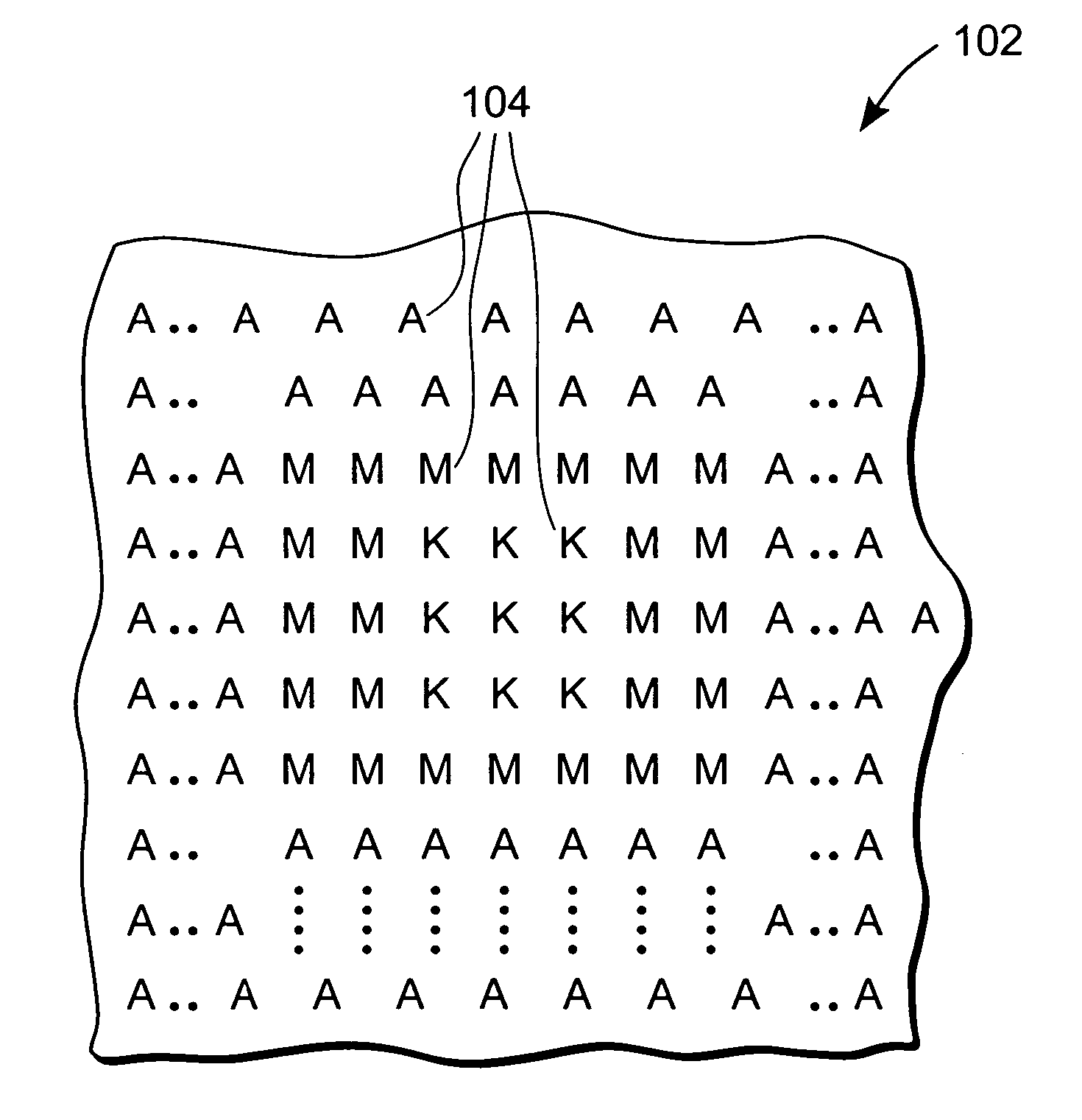
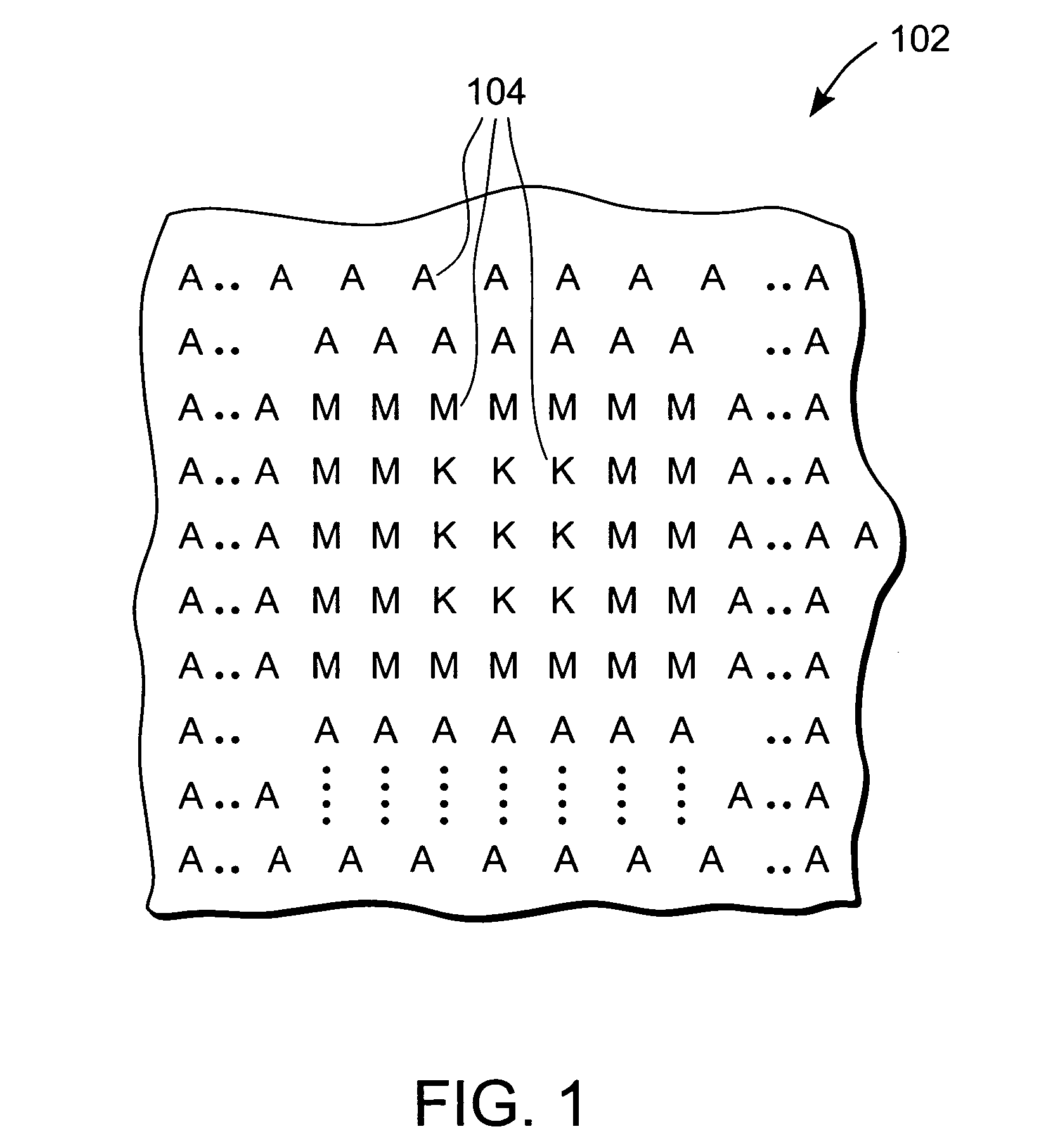
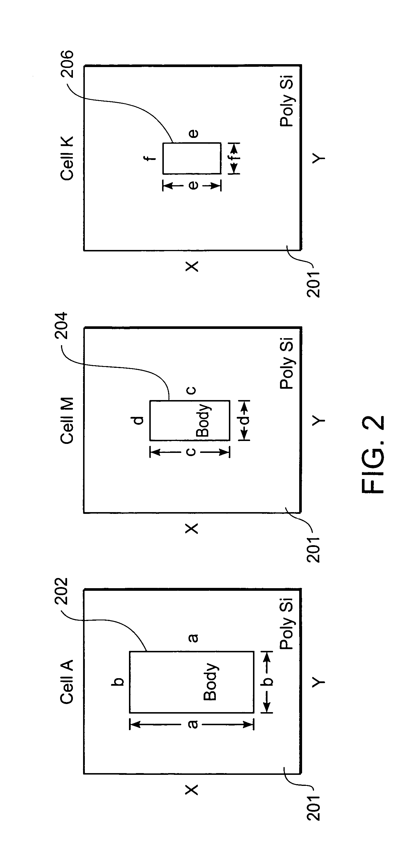
[0026]For purposes of discussion, to distinguish the A cells which are the workhorses of the power device and the B and C cells, the A cells are referred to as the active cells, while the B and C cells are collectively referred to as the peripheral cells. Similarly, the active area 602 (also “active device area”), shown in FIGS. 6A and 6B for example, is distinguished from the other regions (collectively referred to as ancillary regions) such as the guard ring region 604 which typically contains no cells and termination areas 642L, 642R which comprise termination cells. The active area is that area of the device which provides the transistor action, whereas the ancillary regions include structures such as gate vias for distributing the gate current over the area of polysilicon and the guard ring region used around the edge of the die to prevent peripheral voltage breakdown.

[0027]Referring to FIG. 1, the invention provides an active area of a power device in which the constituent act...


PUM


Abstract

A method for making a power device produces a power device comprising active cells having designs that vary depending on where they are located in the active area. Design variations include structural variations and variations in the material used to produce the cells.

Description

CROSS-REFERENCES TO RELATED APPLICATIONS[0001]The present application is a Divisional Application of U.S. application Ser. No. 09 / 764,545, Filed Jan. 17, 2001, now U.S. Pat. No. 6,710,405 which is incorporated by reference herein in its entirety for all purposes.BACKGROUND OF THE INVENTION[0002]The present invention relates to semiconductor devices, and more specifically to semiconductor devices having repeated cell structures. In particular the invention is directed to semiconductor power devices which comprise one or more arrays of active cells (transistors), but is applicable in devices such as semiconductor memories which comprise one or more arrays of repeated active cells, namely, memory cells.[0003]Semiconductor power devices (e.g., metal oxide semiconductor field effect transistors, MOSFETs) are designed and manufactured with a repetitive structure. The repeated structure comprises patterns of one or more repetitive cell (transistor) structures and ancillary elements. FIG. 6...

Claims


Application Information

Patent Timeline
IPC IPC(8): H01L21/8234H01L21/3205H01L21/82H01L27/10H01L29/76H01L29/06H01L29/08H01L29/10H01L29/78
CPCH01L29/0696H01L29/0865H01L29/7802H01L29/1095H01L29/7811H01L29/78
Inventor ZOMMER, NATHANTSUKANOV, VLADIMIR
Owner LITTELFUSE INC
Why Eureka
Try Eureka